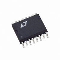
LTC1590CS Linear Technology, LTC1590CS Datasheet - Page 5

LTC1590CS
Manufacturer Part Number
LTC1590CS
Description
IC D/A CONV 12BIT DUAL 16-SOIC
Manufacturer
Linear Technology
Datasheet
1.LTC1590ISPBF.pdf
(12 pages)
Specifications of LTC1590CS
Settling Time
1.5µs
Number Of Bits
12
Data Interface
Serial
Number Of Converters
2
Voltage Supply Source
Single Supply
Power Dissipation (max)
55µW
Operating Temperature
0°C ~ 70°C
Mounting Type
Surface Mount
Package / Case
16-SOIC (3.9mm Width)
Lead Free Status / RoHS Status
Contains lead / RoHS non-compliant
Available stocks
Company
Part Number
Manufacturer
Quantity
Price
Part Number:
LTC1590CS
Manufacturer:
LINEAR/凌特
Quantity:
20 000
TYPICAL PERFORMANCE CHARACTERISTICS
PIN
V
Typically 10V, accepts up to 25V.
R
Normally tied to the output of current to voltage converter
op amp. Typically swings to 10V. Swings from 0V to
– V
OUT1 B, OUT1 A (Pins 3, 6): True Current Output for DAC
A/B. Normally tied to inverting input of current to voltage
converter op amp.
OUT2 B, OUT2 A (Pins 4, 5): Complement Current Output
for DAC A/B. Normally tied to ground.
AGND (Pin 7): Analog Ground Pin. Tie to ground.
DGND (Pin 10): Digital Ground Pin. Tie to ground.
CS/LD (Pin 11): The Serial Interface Enable and Load
Control Input. When CS/LD is low the CLK signal is
REF B
FB B
Midscale Glitch Impulse
U
REF
V
LT1363 OP AMP
C
, R
DD
FB
, V
.
FUNCTIONS
= 30pF
= 5V
FB A
REF A
U
(Pins 2, 8): Feedback Resistors for DAC A/B.
TIME (500ns/DIV)
(Pins 1, 9): Reference Inputs for DAC A/B.
U
W
1590 G11
U
4
3
2
1
0
0
Logic Threshold vs
Supply Voltage
SUPPLY VOLTAGE (V)
5
enabled so the data can be clocked in. When CS/LD is
pulled high, data is loaded from the shift register into the
DAC register, updating the DAC output.
D
on the rising edge of the CLK.
D
latched into the shift register on the rising edge of the serial
clock. Data is loaded as one 24-bit word. The first 12 bits
are for DAC A, MSB-first and the second 12 bits are for
DAC B, MSB-first.
CLK (Pin 14): The Serial Interface Clock Input.
CLR (Pin 15): The Clear Pin for the DAC. Clears both DACs
to zero scale when pulled low. This pin should be tied to
V
V
CC
CC
OUT
IN
5.5V. Requires a bypass capacitor to ground.
10
(Pin 13): The Serial Data Input. Data on the D
for normal operation.
(Pin 16): The Positive Supply Input. 4.5
(Pin 12): The Serial Data Output. Data becomes valid
1590 G04
15
1.0
0.5
0
0
Supply Current vs
Logic Input Voltage
1
INPUT VOLTAGE (V)
2
LTC1590
3
IN
4
pin is
1590 G01
V
5
CC
5


