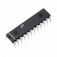
LTC1450CN Linear Technology, LTC1450CN Datasheet

LTC1450CN
Specifications of LTC1450CN
Available stocks
Related parts for LTC1450CN
LTC1450CN Summary of contents
Page 1
... The LTC1450/LTC1450L offer true stand-alone perfor- mance. In addition, the reference output, high and low reference inputs and gain setting resistor are brought to pins for maximum flexibility. , LTC and LT are registered trademarks of Linear Technology Corporation. LTC1450: 5V LTC1450L REFOUT REFHI ...
Page 2
... Using External Reference, LTC1450/LTC1450L Using Internal Reference, LTC1450L LTC1450L LTC1450 0 I 100 A, LTC1450L OUT LTC1450 REFOUT Shorted to GND U W INFORMATION ORDER PART TOP VIEW NUMBER 1 24 LDAC 2 23 CLR LTC1450CG 3 22 X1/X2 LTC1450CN OUT LTC1450IG LTC1450IN 6 19 REFOUT 7 REFHI LTC1450LCG REFLO LTC1450LCN 9 GND 16 LTC1450LIG ...
Page 3
ELECTRICAL CHARACTERISTICS REFOUT = REFHI, REFLO = GND = X1/X2, T SYMBOL PARAMETER Reference Input (REFLO = GND) REFHI Input Range REFHI Input Resistance REFHI Input Capacitance Power Supply V Positive Supply Voltage CC I Supply Current CC Op Amp ...
Page 4
LTC1450/LTC1450L ELECTRICAL CHARACTERISTICS V = 4.5V to 5.5V (LTC1450 2.7V to 3.6V (LTC1450L SYMBOL PARAMETER Switching Characteristics (Note (MSB or LSB) Pulse Width Pulse Width ...
Page 5
W U TYPICAL PERFORMANCE CHARACTERISTICS LTC1450L Supply Current vs Logic Input Voltage 1600 ALL LOGIC INPUTS 1400 TIED TOGETHER 1200 1000 800 600 400 200 0 0 0.3 0.6 0.9 1.2 1.5 1.8 2.1 2.4 2.7 ...
Page 6
LTC1450/LTC1450L W U TYPICAL PERFORMANCE CHARACTERISTICS LTC1450 Midscale Transition Data = 2048 to 2047 V OUT 20mV/DIV LDAC 5V 0V 500ns/DIV 1450/50L G13 Output Voltage Full-Scale Settling 5V DATA IN 0V 000 TO FFF OUT 1mV/DIV OUTPUT ...
Page 7
PIN FUNCTIONS WR (Pin 1): Write Input (Active Low). Used with CSMSB and/or CSLSB to load data into the input latches. While WR and CSMSB and/or CSLSB are held low the enabled input latches are transparent. The ...
Page 8
LTC1450/LTC1450L U DIGITAL INTERFACE TRUTH TABLE CLR CSMSB CSLSB ...
Page 9
U U DEFI ITIO S Resolution (n): Resolution is defined as the number of digital input bits (n). It defines the number of DAC output n states (2 ) that divide the full-scale range. The resolution does not imply linearity. ...
Page 10
LTC1450/LTC1450L U OPERATION Parallel Interface The data on the input of the DAC is loaded into the DAC’s input latches when Chip Select (CSLSB and/or CSMSB) and WR are at a logic low. The data that is loaded into the ...
Page 11
U TYPICAL APPLICATIONS FROM P AND DECODE LOGIC SYSTEM RESET D IN FROM P DATA BUS FROM P AND DECODE LOGIC FROM SYSTEM RESET N Filter V to Lower Output Noise (0.18mV REF 5V 0 FROM P ...
Page 12
LTC1450/LTC1450L U TYPICAL APPLICATIONS 5V 0 FROM P DATA (0:11) V DATA BUS CSLSB CSMSB FROM P AND DECODE LOGIC WR LDAC FROM CLR SYSTEM RESET Digitally Programmable Bilateral Current Source/Sink ...
Page 13
U TYPICAL APPLICATIONS 4-Quadrant Multiplying DAC Application This application shows the LTC1450L configured as a single supply 4-quadrant multiplying DAC. It uses a 5V supply and only one external component resistor tied from REFOUT to ground. (The LTC1450 ...
Page 14
LTC1450/LTC1450L PACKAGE DESCRIPTION 0.205 – 0.212** (5.20 – 5.38) 0.005 – 0.009 0.022 – 0.037 (0.13 – 0.22) (0.55 – 0.95) * DIMENSIONS DO NOT INCLUDE MOLD FLASH. MOLD FLASH SHALL NOT EXCEED 0.006" (0.152mm) PER SIDE ** DIMENSIONS DO ...
Page 15
... MOLD FLASH OR PROTRUSIONS SHALL NOT EXCEED 0.010 INCH (0.254mm) Information furnished by Linear Technology Corporation is believed to be accurate and reliable. However, no responsibility is assumed for its use. Linear Technology Corporation makes no represen- tation that the interconnection of its circuits as described herein will not infringe on existing patent rights. ...
Page 16
... Wide Latched Input 8-Pin SO and PDIP : 499-3977 = 4.5V TO 5.5V 4.095V CC OUT = 2.7V to 5.5V 2.5V CC OUT = 4.5V to 5.5V 4.095V CC OUT = 2.7V to 5.5V 2.5V CC OUT = 4.5V to 5.5V 4.095V CC OUT = 2.7V to 5.5V 2.5V CC OUT LT/GP 0896 7K • PRINTED IN USA LINEAR TECHNOLOGY CORPORATION 1996 ...


