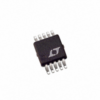
LTC2634IMSE-HMX10#TRPBF Linear Technology, LTC2634IMSE-HMX10#TRPBF Datasheet - Page 10

LTC2634IMSE-HMX10#TRPBF
Manufacturer Part Number
LTC2634IMSE-HMX10#TRPBF
Description
IC DAC 10BIT QUAD 2.5V 10-MSOP
Manufacturer
Linear Technology
Datasheet
1.LTC2634IMSE-LZ10PBF.pdf
(30 pages)
Specifications of LTC2634IMSE-HMX10#TRPBF
Settling Time
3.8µs
Number Of Bits
10
Data Interface
MICROWIRE™, Serial, SPI™
Number Of Converters
4
Voltage Supply Source
Single Supply
Power Dissipation (max)
1.8mW
Operating Temperature
-40°C ~ 85°C
Mounting Type
Surface Mount
Package / Case
10-MSOP Exposed Pad, 10-HMSOP, 10-eMSOP
Lead Free Status / RoHS Status
Lead free / RoHS Compliant
Available stocks
Company
Part Number
Manufacturer
Quantity
Price
LTC2634
electrical characteristics
temperature range, otherwise specifications are at T
LTC2634-HMI12/-HMI10/-HMI8/-HMX12/-HMX10/-HMX8/-HZ12/-HZ10/-HZ8 (V
SYMBOL
t
t
t
t
t
t
t
t
t
t
t
t
Note 1: Stresses beyond those listed under Absolute Maximum Ratings
may cause permanent damage to the device. Exposure to any Absolute
Maximum Rating condition for extended periods may affect device
reliability and lifetime.
Note 2: All voltages are with respect to GND.
Note 3: High temperatures degrade operating lifetimes. Operating lifetime
is derated at temperatures greater than 105°C. Operating at temperatures
above 90°C and with V
than 73mV/ms.
Note 4: Linearity and monotonicity are defined from code k
2
rounded to the nearest whole code. For V
and linearity is defined from code 26 to code 4,095. For V
N = 12, k
0
1
2
3
4
5
6
7
8
9
10
11
12
N
– 1, where N is the resolution and k
L
= 16 and linearity is defined from code 16 to code 4,095.
PARAMETER
SDI Valid to SCK Setup
SDI Valid to SCK Hold
SCK High Time
SCK Low Time
CS/LD Pulse Width
LSB SCK High to CS/LD High
CS/LD Low to SCK High
CLR Pulse Width
LDAC Pulse Width
CS/LD High to SCK Positive Edge
SCK Frequency
CS/LD High to LDAC High or Low Transition
SDO Propagation Delay from SCK Falling Edge
CC
> 4V requires V
L
is given by k
CC
FS
slew rates to be no greater
= 2.5V and N = 12, k
L
= 0.016 • (2
FS
L
A
= 4.096V and
to code
= 25°C. V
CONDITIONS
50% Duty Cycle
C
LOAD
V
L
CC
= 26
N
/ V
The
= 4.5V to 5.5V
= 10pF
FS
),
l
CC
denotes the specifications which apply over the full operating
= 4.5V to 5.5V, V
Note 5: Inferred from measurement at code 16 (LTC2634-12), code 4
(LTC2634-10) or code 1 (LTC2634-8), and at full-scale.
Note 6: This IC includes current limiting that is intended to protect the
device during momentary overload conditions. Junction temperature can
exceed the rated maximum during current limiting. Continuous operation
above the specified maximum operating junction temperature may impair
device reliability.
Note 7: Digital inputs at 0V or V
Note 8: Guaranteed by design and not production tested.
Note 9: Internal Reference mode. DAC is stepped 1/4 scale to 3/4 scale
and 3/4 scale to 1/4 scale. Load is 2kΩ in parallel with 100pF to GND.
Note 10: Temperature coefficient is calculated by dividing the maximum
change in output voltage by the specified temperature range.
FS
= 4.096V)
OUT
unloaded unless otherwise specified.
l
l
l
l
l
l
l
l
l
l
l
l
l
CC
MIN
200
10
20
15
4
4
9
9
7
7
7
.
TYP
MAX
50
20
UNITS
2634fc
MHz
ns
ns
ns
ns
ns
ns
ns
ns
ns
ns
ns
ns


