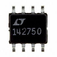
LTC1427CS8-50#TR Linear Technology, LTC1427CS8-50#TR Datasheet - Page 6

LTC1427CS8-50#TR
Manufacturer Part Number
LTC1427CS8-50#TR
Description
IC DAC 10BIT SMBUS MICRPWR 8SOIC
Manufacturer
Linear Technology
Datasheet
1.LTC1427CS8-50PBF.pdf
(8 pages)
Specifications of LTC1427CS8-50#TR
Number Of Bits
10
Data Interface
Serial
Number Of Converters
1
Voltage Supply Source
Single Supply
Power Dissipation (max)
550µW
Operating Temperature
0°C ~ 70°C
Mounting Type
Surface Mount
Package / Case
8-SOIC (3.9mm Width)
Lead Free Status / RoHS Status
Contains lead / RoHS non-compliant
Settling Time
-
Available stocks
Company
Part Number
Manufacturer
Quantity
Price
APPLICATIONS
Digital Interface
The LTC1427-50 communicates with an SMBus host
using the standard 2-wire SMBus interface. The Timing
Diagram shows the signals on the SMBus. The SCL and
SDA bus lines must be high when the bus is not in use.
External pull-up resistors or current sources are required
at these lines.
The LTC1427-50 is a receive-only (slave) device. The
master must apply the following Write Byte protocol to
communicate with the LTC1427-50:
S = Start Condition, WR = Write Bit, A = Acknowledge Bit, P = Stop Condition
LTC1427-50
6
TI I G DIAGRA S
SDA
I
AD1
AD0
SCL
OUT
S Slave Address WR
1
W
S = START
P = STOP
* = OPTIONAL
S
U
7
0
1
1
2
SDA
SCL
SMBUS ADDRESS
0
3
1
STOP
U
1
4
A
1
t
BUF
1
5
Command Byte
INFORMATION
START
U
1
6
W
8
1
7
t
LOW
t
SMBus Write Byte Protocol, with SMBus Address = 0101111B,
HD:STA
8
Command Byte = 0XXXXX11B and Data Byte = 11111111B
W
9
1
A Data Byte
t
r
10
11
X
8
t
U
Timing for SMBus Interface
HD:DAT
12
X
COMMAND BYTE
t
HIGH
Operating Sequence
13
1 1
A P
X
14
X
t
f
15
X
The master initiates communication with the LTC1427-50
with a START condition (see SMBus Operating Sequence)
and a 7-bit address followed by the write bit = 0. The
LTC1427-50 acknowledges and the master delivers the
command byte. The LTC1427-50 acknowledges and latches
the active bits of the command byte into register A (see
Block Diagram) at the falling edge of the acknowledge
pulse. The master sends the data byte and the LTC1427-
50 acknowledges the data byte. The data byte and last two
output bits from register A are latched into register C at the
falling edge of the final acknowledge pulse and the DAC
current output assumes the new 10-bit data value (see
Block Diagram). A STOP condition is optional. The com-
16
1
t
t
SU:DAT
SU:STA
17
1
18
START
19
1
20
1
t
HD:STA
21
1
DATA BYTE
22
1
t
SU:STO
1
23
24
1
25
1
STOP
26
1
1427 TD01
27
1427 TD02
*
P
ZERO-SCALE
CURRENT
V
GND
V
GND
FULL-SCALE
CURRENT
CC
CC


