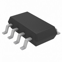
LTC2640HTS8-LM10#TRMPBF Linear Technology, LTC2640HTS8-LM10#TRMPBF Datasheet - Page 19

LTC2640HTS8-LM10#TRMPBF
Manufacturer Part Number
LTC2640HTS8-LM10#TRMPBF
Description
IC DAC 10BIT VOUT W/REF TSOT23-8
Manufacturer
Linear Technology
Datasheet
1.LTC2640CTS8-HM10TRMPBF.pdf
(24 pages)
Specifications of LTC2640HTS8-LM10#TRMPBF
Settling Time
3.8µs
Number Of Bits
10
Data Interface
Serial
Number Of Converters
1
Voltage Supply Source
Single Supply
Power Dissipation (max)
450µW
Operating Temperature
-40°C ~ 125°C
Mounting Type
Surface Mount
Package / Case
TSOT-23-8, TSOT-8
Lead Free Status / RoHS Status
Lead free / RoHS Compliant
Available stocks
Company
Part Number
Manufacturer
Quantity
Price
OPERATION
Power-Down Mode
For power-constrained applications, the LTC2640’s power-
down mode can be used to reduce the supply current
whenever the DAC output is not needed. When in power-
down, the buffer amplifi er, bias circuit, and reference
circuit are disabled and draw essentially zero current. The
DAC output is put into a HIGH-impedance state, and the
output pin is passively pulled to ground through a 200k
resistor. Input and DAC register contents are not disturbed
during power-down.
The DAC can be put into power-down mode by using
command 0100. The supply current is reduced to 1.8μA
maximum (C and I grades) and the REF pin becomes HIGH
impedance (typically > 1GΩ).
Normal operation resumes after executing any command
that includes a DAC update, as shown in Table 1. The
DAC is powered up and its voltage output is updated.
Normal settling is delayed while the bias, reference, and
amplifi er circuits are re-enabled. When the REF pin output
is bypassed to GND with 1nF or less, the power-up delay
time is 20μs for settling to 12-bits. This delay increases
to 200μs for 0.33μF, and 10ms for 10μF.
Voltage Output
The LTC2640’s integrated rail-to-rail amplifi er has guar-
anteed load regulation when sourcing or sinking up to
10mA at 5V, and 5mA at 3V.
Load regulation is a measure of the amplifi er’s ability to
maintain the rated voltage accuracy over a wide range of
load current. The measured change in output voltage per
change in forced load current is expressed in LSB/mA.
DC output impedance is equivalent to load regulation, and
may be derived from it by simply calculating a change in
units from LSB/mA to ohms. The amplifi er’s DC output
impedance is 0.1Ω when driving a load well away from
the rails.
When drawing a load current from either rail, the output
voltage headroom with respect to that rail is limited by
the 50Ω typical channel resistance of the output devices
(e.g., when sinking 1mA, the minimum output voltage is
50Ω • 1mA, or 50mV). See the graph “Headroom at Rails
vs. Output Current” in the Typical Performance Charac-
teristics section.
The amplifi er is stable driving capacitive loads of up to
500pF.
Rail-to-Rail Output Considerations
In any rail-to-rail voltage output device, the output is limited
to voltages within the supply range.
Since the analog output of the DAC cannot go below ground,
it may limit the lowest codes, as shown in Figure 4b.
Similarly, limiting can occur near full-scale when the REF
pin is tied to V
(FSE) is positive, the output for the highest codes limits
at V
occur if V
Offset and linearity are defi ned and tested over the region
of the DAC transfer function where no output limiting can
occur.
Board Layout
The PC board should have separate areas for the analog and
digital sections of the circuit. A single, solid ground plane
should be used, with analog and digital signals carefully
routed over separate areas of the plane. This keeps digital
signals away from sensitive analog signals and minimizes
the interaction between digital ground currents and the
analog section of the ground plane. The resistance from
the LTC2640 GND pin to the ground plane should be as
low as possible. Resistance here will add directly to the
effective DC output impedance of the device (typically
0.1Ω). Note that the LTC2640 is no more susceptible to
CC
, as shown in Figure 4c. No full-scale limiting can
REF
is less than V
CC
. If V
REF
= V
CC
CC
and the DAC full-scale error
– FSE.
LTC2640
19
2640fb


