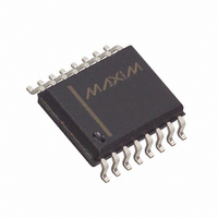
MAX536BEWE+ Maxim Integrated Products, MAX536BEWE+ Datasheet - Page 20

MAX536BEWE+
Manufacturer Part Number
MAX536BEWE+
Description
IC DAC 12BIT QUAD CALIB 16-SOIC
Manufacturer
Maxim Integrated Products
Datasheet
1.MAX536BCWE.pdf
(24 pages)
Specifications of MAX536BEWE+
Settling Time
3µs
Number Of Bits
12
Data Interface
Serial
Number Of Converters
4
Voltage Supply Source
Dual ±
Power Dissipation (max)
762mW
Operating Temperature
-40°C ~ 85°C
Mounting Type
Surface Mount
Package / Case
16-SOIC (0.300", 7.5mm Width)
Lead Free Status / RoHS Status
Lead free / RoHS Compliant
Calibrated, Quad, 12-Bit
Voltage-Output DACs with Serial Interface
SS is an input intended for use in a multimaster environ-
ment. However, SS or unused PORT D bit RXD, TXD, or
possibly MISO (if DAC readback is not used) should be
configured as a general-purpose output and used as CS by
setting the appropriate Data Direction Register bit.
The SPCR configuration (memory location $1028) is shown
below:
**Depends on µP clock frequency.
Always configure the 68HC11 as the “master” controller
and the MAX536/MAX537 as the “slave” device.
When MSTR = 1 in the SPCR, a write to the Serial
Peripheral Data I/O Register (SPDR), located at memory
location $102A, initiates the transmission/reception of
data. The data transfer is monitored and the appropri-
ate flags are set in the Serial Peripheral Status
Register (SPSR).
The SPSR configuration is shown below:
An example of 68HC11 programming code for a
two-byte SPI transfer to the MAX536/MAX537 is given in
Table 4. SS is used for CS, the high byte of MAX536/
MAX537 digital data is stored in memory location $0100,
and the low byte is stored in memory location $0101.
When using Microwire, refer to the section on Inter-
facing to the M68HC11 for guidance, since Microwire
can be considered similar to SPI when CPOL = 0 and
CPHA = 0. When interfacing to Intel’s 80C51/80C31
microcontroller family, use bit-pushing to configure a
desired port as the MAX536/MAX537 interface port. Bit-
pushing involves arbitrarily assigning I/O port bits as
interface control lines, and then writing to the port each
time a signal transition is required.
20
*U = Unknown
BIT
BIT
7
NAME
SPIF WCOL
RESET CONDITIONS
0
7
NAME
SPIE SPE DWOM MSTR CPOL CPHA SPR1 SPR0
SETTING AFTER RESET
0
SETTING FOR TYPICAL SPI COMMUNICATION
0
______________________________________________________________________________________
6
0
1
6
0
5
0
0
Interfacing to Other Controllers
5
0
–
MODF
4
0
1
4
0
3
0
0
3
0
–
2
1
0
2
–
0
U
0
1
**
*
1
–
0
1
U
0
**
*
0
0
–
NOTE: 1LSB = (V
For a unipolar output, the output voltages and the reference
inputs are the same polarity. Figure 10 shows the
MAX536/MAX537 unipolar output circuit, which is also the typ-
ical operating circuit. Table 5 lists the unipolar output codes.
The MAX536/MAX537 outputs can be configured for
bipolar operation using Figure 11’s circuit. One op amp
and two resistors are required per DAC. With R1 = R2:
where N
input code. Table 6 shows digital codes and corre-
sponding output voltages for Figure 11’s circuit.
Table 5. Unipolar Code Table
Table 6. Bipolar Code Table
1 1 1 1
1 0 0 0
0 1 1 1
0 0 0 0
0 0 0 0
1000
1 1 1 1
1 0 0 0
0 1 1 1
0 0 0 0
0 0 0 0
1000
MSB
MSB
DAC CONTENTS
DAC CONTENTS
B
1 1 1 1
0 0 0 0
1 1 1 1
0 0 0 0
0 0 0 0
1 1 1 1
0 0 0 0
1 1 1 1
0 0 0 0
0 0 0 0
0000
0000
is the numeric value of the DAC’s binary
V
OUT
REF
1 1 1 1
0 0 0 0
1 1 1 1
0 0 0 1
0 0 0 0
= V
1 1 1 1
0 0 0 0
1 1 1 1
0 0 0 1
0 0 0 0
0001
) (
0001
LSB
LSB
4096
REF
1
)
[(2N
B
+V
-V
/ 4096) - 1]
REF
ANALOG OUTPUT
ANALOG OUTPUT
REF
Unipolar Output
+V
+V
+V
+V
+V
+V
-V
-V
Bipolar Output
( ——— ) = ————
REF
REF
( ——— ) = -V
REF
REF
REF
REF
REF
REF
2048
4096
2048
2048
0V
( ——— )
( ——— )
0V
( ——— )
( ——— )
( ——— )
( ——— )
( ——— )
( ——— )
2047
2048
2048
2047
2048
4095
4096
2047
4096
4096
2048
4096
2049
1
1
1
+V
REF
REF
2


