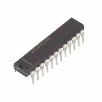
MX7837JN+ Maxim Integrated Products, MX7837JN+ Datasheet - Page 2

MX7837JN+
Manufacturer Part Number
MX7837JN+
Description
IC DAC 12BIT DL MULT 24-DIP
Manufacturer
Maxim Integrated Products
Datasheet
1.MX7837JN.pdf
(12 pages)
Specifications of MX7837JN+
Settling Time
4µs
Number Of Bits
12
Data Interface
Parallel
Number Of Converters
2
Voltage Supply Source
Dual ±
Power Dissipation (max)
1.07W
Operating Temperature
0°C ~ 70°C
Mounting Type
Through Hole
Package / Case
24-DIP (0.300", 7.62mm)
Lead Free Status / RoHS Status
Lead free / RoHS Compliant
ABSOLUTE MAXIMUM RATINGS
V
V
V
AGNDA, AGNDB to DGND.........................-0.3V to (V
V
R
Digital Inputs to DGND ...............................-0.3V to (V
Continuous Power Dissipation (T
Complete, Dual, 12-Bit
Multiplying DACs
ELECTRICAL CHARACTERISTICS
(V
V
Note 1: If V
Stresses beyond those listed under “Absolute Maximum Ratings” may cause permanent damage to the device. These are stress ratings only, and functional
operation of the device at these or any other conditions beyond those indicated in the operational sections of the specifications is not implied. Exposure to
absolute maximum rating conditions for extended periods may affect device reliability.
2
Resolution
OUTA
Narrow Plastic DIP (derate 13.33mW/°C above +70°C)....1067mW
SO (derate 11.76mW/°C above +70°C) .........................941mW
Narrow CERDIP (derate 12.50mW/°C above +70°C) ..1000mW
Relative Accuracy
Differential Nonlinearity
Zero-Code Offset Error
Gain Error
V
V
Matching
Input High Voltage
Input Low Voltage
Input Current
Input Capacitance (Note 4)
DC Output Impedance
Short-Circuit Current
DD
SS
REFA
FBA
OUT
STATIC PERFORMANCE (Note 3)
REFERENCE INPUTS
DIGITAL INPUTS
ANALOG OUTPUTS
DD
REF
REFA
to DGND, AGNDA, AGNDB (Note 1) ..............+0.3V to -17V
_______________________________________________________________________________________
to DGND, AGNDA, AGNDB ............................-0.3V to +17V
, R
, V
connected to R
= 11.4V to 16.5V, V
, V
Input Resistance
FBB
PARAMETER
, V
REFB
OUTB
If this possibility exists, a Schottky diode connected between V
REFB
to AGNDA, AGNDB .......(V
SS
to AGNDA, AGNDB .. (V
to AGNDA, AGNDB .....(V
is open-circuited with V
Resistance
FB
(MX7837), T
SS
= -11.4V to -16.5V, AGNDA = AGNDB = DGND = 0V, V
SYMBOL
A
V
DNL
V
INL
= +70°C)
INH
N
INL
A
DD
= T
SS
SS
SS
and either AGND applied, the V
- 0.3V) to (V
- 0.3V) to (V
MIN
- 0.3V) to (V
MX78_7J/A/S
MX78_7K/B/T
Guaranteed monotonic
Loaded with all 0s,
tempco =
Loaded with all 1s,
tempco = ±2ppm
Digital inputs at 0V and V
V
OUT
to T
of FSR/°C typ
±5µV/°C typ
connected to AGND
MAX
, unless otherwise noted.) (Note 2)
DD
DD
DD
DD
DD
+ 0.3V)
+ 0.3V)
+ 0.3V)
+ 0.3V)
+ 0.3V)
CONDITIONS
T
T
T
T
A
A
A
A
= T
= T
= +25°C
= +25°C
MIN
MIN
DD
SS
Operating Temperature Ranges:
Storage Temperature Range ............................ -65°C to +150°C
Lead Temperature (soldering, 10sec) .............................+300°C
SS
MX78_7J_/K_ ........................................................0°C to +70°C
MX78_7A_/B_ .................................................. -40°C to +85°C
MX78_7SQ/TQ ............................................... -55°C to +125°C
and GND ensures the maximum ratings will be observed.
to T
to T
pin will float positive exceeding the Absolute Maximum Ratings .
MAX
MAX
MX78_7J/A
MX78_7K/B
MX78_7S/T
MX78_7J/A/S
MX78_7K/B/T
MX78_7J/A/S
MX78_7K/B/T
REFA
= V
REFB
MIN
2.4
12
8
= +10V, R
±0.5
TYP
0.2
10
15
L
= 2kΩ, C
MAX
±1/2
0.8
±1
±1
±2
±4
±3
±5
±5
±2
±7
±4
13
±3
±1
8
L
= 100pF,
UNITS
LSB
LSB
LSB
Bits
mA
mV
kΩ
µA
pF
%
Ω
V


