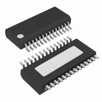
MAX5186BEEI+ Maxim Integrated Products, MAX5186BEEI+ Datasheet - Page 7

MAX5186BEEI+
Manufacturer Part Number
MAX5186BEEI+
Description
IC DAC 8BIT DUAL 40MHZ 28-QSOP
Manufacturer
Maxim Integrated Products
Datasheet
1.MAX5186BEEI.pdf
(14 pages)
Specifications of MAX5186BEEI+
Settling Time
25µs
Number Of Bits
8
Data Interface
Parallel
Number Of Converters
2
Voltage Supply Source
Analog and Digital
Operating Temperature
-40°C ~ 85°C
Mounting Type
Surface Mount
Package / Case
28-QSOP
Lead Free Status / RoHS Status
Lead free / RoHS Compliant
Power Dissipation (max)
-
15–20
PIN
10
11
12
13
14
21
22
23
24
25
26
27
28
1
2
3
4
5
6
7
8
9
DACEN
OUT1P
OUT1N
OUT2N
OUT2P
CREF1
NAME
DGND
DGND
D1–D6
DGND
REFR
REFO
CREF2
AGND
AV
DV
N.C.
REN
CLK
PD
CS
D0
D7
DD
DD
_______________________________________________________________________________________
Reference Bias Bypass, DAC1
Positive Analog Output, DAC1. Current output for MAX5186; voltage output for MAX5189.
Negative Analog Output, DAC1. Current output for MAX5186; voltage output for MAX5189.
Analog Ground
Analog Positive Supply, 2.7V to 3.3V
DAC Enable, Digital Input
0: Enter DAC standby mode with PD = DGND.
1: Power-up DAC with PD = DGND.
X: Enter shutdown mode with PD = DV
Power-Down Select
0: Enter DAC standby mode (DACEN = DGND) or power-up DAC (DACEN = DV
1: Enter shutdown mode.
Active-Low Chip Select
Clock input
No Connect. Do not connect to this pin.
Active-Low Reference Enable. Connect to DGND to activate on-chip 1.2V reference.
Digital Ground
Digital Ground
Data Bit D0 (LSB)
Data Bits D1–D6
Data Bit D7 (MSB)
Digital Supply, 2.7V to 3.3V
Digital Ground
Reference Input
Reference Output
Negative Analog Output, DAC2. Current output for MAX5186; voltage output for MAX5189.
Positive Analog Output, DAC2. Current output for MAX5186; voltage output for MAX5189.
Reference Bias Bypass, DAC2
Dual, 8-Bit, 40MHz, Current/Voltage,
Simultaneous-Output DACs
DD
(X = don’t care).
FUNCTION
DD
Pin Description
).
7


