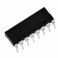
DAC8420FPZ Analog Devices Inc, DAC8420FPZ Datasheet

DAC8420FPZ
Specifications of DAC8420FPZ
Related parts for DAC8420FPZ
DAC8420FPZ Summary of contents
Page 1
FEATURES Guaranteed monotonic over temperature Excellent matching between DACs Unipolar or bipolar operation Buffered voltage outputs High speed serial digital interface Reset-to-zero scale or midscale Wide supply range only to ±15 V Low power consumption (35 mW maximum) ...
Page 2
DAC8420 TABLE OF CONTENTS Features .............................................................................................. 1 Applications....................................................................................... 1 Functional Block Diagram .............................................................. 1 General Description ......................................................................... 1 Revision History ............................................................................... 2 Specifications..................................................................................... 3 Electrical Characteristics............................................................. 3 Absolute Maximum Ratings............................................................ 6 Thermal Resistance ...................................................................... 6 ESD Caution.................................................................................. 6 Pin Configurations ...
Page 3
SPECIFICATIONS ELECTRICAL CHARACTERISTICS @ V = +5.0 V ± 5 VREFHI 2 otherwise noted. Table 1. Parameter STATIC ACCURACY Integral Linearity E Grade Integral Linearity E Grade Integral Linearity F Grade Integral Linearity ...
Page 4
DAC8420 Parameter SUPPLY CHARACTERISTICS Power Supply Sensitivity Positive Supply Current Negative Supply Current Power Dissipation 1 Typical values indicate performance measured at 25°C. 2 All supplies can be varied ±5% and operation is guaranteed. Device is tested with V 3 ...
Page 5
V = +15.0 V ± 5 −15.0 V ± 5 Table 2. Parameter Symbol STATIC ACCURACY Integral Linearity E Grade INL Integral Linearity F Grade INL Differential Linearity DNL Zero-Scale Error ZSE Full-Scale Error ...
Page 6
DAC8420 ABSOLUTE MAXIMUM RATINGS T = 25°C, unless otherwise noted. A Table 3. Parameter Rating V to GND −0.3 V, +18 GND +0.3 V, −18 −0.3 V, +36 ...
Page 7
DATA LOAD SEQUENCE CS t CSS SDI A1 A0 CLK t LD1 DATA LOAD TIMING DS DH SDI CLK CSH CS t LD2 LD VOUTx +15V 1N4001 –10V 1N4001 +10V 1N4001 –15V ...
Page 8
DAC8420 PIN CONFIGURATIONS AND FUNCTION DESCRIPTIONS VDD 1 16 VOUTD 2 15 VOUTC 3 DAC8420 14 VREFLO TOP VIEW 4 13 (Not to Scale) VREFHI 5 12 VOUTB 6 11 VOUTA 7 10 VSS CONNECT ...
Page 9
Table 6. Control Function Logic Table 1 1 CLK CS LD CLR 2 NC High High Low 2 NC High High Low ↑ High High ↑ Low High High ↑ Low High High ↓ 2 High NC (↑) ...
Page 10
DAC8420 TYPICAL PERFORMANCE CHARACTERISTICS 0.3 0.2 0.1 0 –0.1 –0.2 –0.3 –6 –4 – (V) VREFHI Figure 6. DNL vs. V (±15 V) VREFHI 0.10 0.05 0 –0.05 –0.10 –0.15 –0.20 –0.25 –0.30 1.5 2.0 ...
Page 11
V = +15V –15V 0 VREFHI V VREFLO 0 –0.1 DAC C –0.2 DAC A –0.3 DAC B –0.4 –0.5 –0.6 –75 –50 – ° TEMPERATURE ( C) Figure 12. ...
Page 12
DAC8420 1.5 1.0 0 –0 VREFHI V VREFLO –1.0 0 500 1000 1500 2000 2500 3000 DIGITAL INPUT CODE Figure 18. I vs. Code VREFHI –2.50µV LD 1.22mV 1 LSB 0mV –10.25mV ...
Page 13
LD CLR +5V/DIV +25° +15V –15V +10V VREFHI V = –10V VREFLO –25V –33.6µs 20µs/DIV 1.9 SR RISE FALL µs Figure 24. Slew Rate ...
Page 14
DAC8420 THEORY OF OPERATION INTRODUCTION The DAC8420 is a quad, voltage-output 12-bit DAC with a serial digital input capable of operating from a single 5 V supply. The straightforward serial interface can be connected directly to most popular microprocessors and ...
Page 15
Table 9. Analog Output Code DAC Data-Word (Hex) 0xFFF 0x801 0x800 0x7FF 0x000 V OUT − ( VREFHI VREFLO ) + × VREFLO 4095 4096 − ( VREFHI VREFLO ) + × VREFLO 2049 4096 − ( VREFHI VREFLO ) ...
Page 16
DAC8420 VREFHI INPUT REQUIREMENTS The DAC8420 utilizes a unique, patented DAC switch driver circuit that compensates for different supply, reference voltage, and digital code inputs. This ensures that all DAC ladder switches are always biased equally, ensuring excellent linearity under ...
Page 17
APPLICATIONS POWER SUPPLY BYPASSING AND GROUNDING In any circuit where accuracy is important, careful consid- eration of the power supply and ground return layout helps to ensure the rated performance. The DAC8420 has a single ground pin that is internally ...
Page 18
DAC8420 is 16 mV. Thus, the best single-supply operation is obtained with the output load connected to ground, so the output stage does not have to sink current. Like all amplifiers, the DAC8420 output buffers do generate voltage noise, 52 ...
Page 19
For a single 5 V supply limited to at most 2.5 V, and VREFHI must always be at least 2.5 V less than the positive supply to ensure linearity of the device. For these applications, the REF43 is ...
Page 20
DAC8420 5V SUPPLY REF43 0.1µF 4 GND V OUT 6 DAC8420 DIGITAL CONTROLS DIGITAL INPUTS DUAL WINDOW COMPARATOR Often a comparator is needed to signal an out-of-range warning. Combining the DAC8420 ...
Page 21
DAC8420 TO M68HC11 INTERFACE ASSEMBLY PROGRAM * M68HC11 Register Definitions PORTC EQU $1003 Port C control register * “0,0,0,0;0,CLSEL,CLR,CS” DDRC EQU $1007 Port C data direction PORTD EQU $1008 Port D data register * “0,0,LD,SCLK;SDI,0,0,0” DDRD EQU $1009 Port D ...
Page 22
DAC8420 OUTLINE DIMENSIONS 0.210 (5.33) MAX 0.150 (3.81) 0.130 (3.30) 0.115 (2.92) 0.022 (0.56) 0.018 (0.46) 0.014 (0.36) 0.30 (0.0118) 0.10 (0.0039) COPLANARITY 0.10 0.800 (20.32) 0.790 (20.07) 0.780 (19.81 0.280 (7.11) 0.250 (6.35) 1 0.240 (6.10) 8 ...
Page 23
... DAC8420ESZ −40°C to +85°C 2 DAC8420ESZ-REEL −40°C to +85°C DAC8420FP −40°C to +85°C 2 DAC8420FPZ −40°C to +85°C DAC8420FQ −40°C to +85°C DAC8420FS −40°C to +85°C DAC8420FS-REEL −40°C to +85°C 2 DAC8420FSZ −40°C to +85°C ...
Page 24
DAC8420 NOTES ©2007 Analog Devices, Inc. All rights reserved. Trademarks and registered trademarks are the property of their respective owners. C00275-0-5/07(B) Rev Page ...


