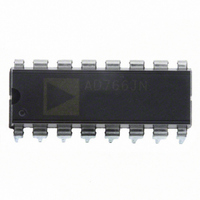
AD766JNZ Analog Devices Inc, AD766JNZ Datasheet - Page 6

AD766JNZ
Manufacturer Part Number
AD766JNZ
Description
IC DAC 16BIT W/VREF 16-DIP
Manufacturer
Analog Devices Inc
Series
DACPORT®r
Datasheet
1.AD766JNZ.pdf
(8 pages)
Specifications of AD766JNZ
Data Interface
Serial
Settling Time
1.5µs
Number Of Bits
16
Number Of Converters
1
Voltage Supply Source
Analog and Digital, Dual ±
Power Dissipation (max)
300mW
Operating Temperature
-40°C ~ 85°C
Mounting Type
Through Hole
Package / Case
16-DIP (0.300", 7.62mm)
Resolution (bits)
16bit
Sampling Rate
390kSPS
Input Channel Type
Serial
Supply Current
-14mA
Digital Ic Case Style
DIP
No. Of Pins
16
Lead Free Status / RoHS Status
Lead free / RoHS Compliant
Available stocks
Company
Part Number
Manufacturer
Quantity
Price
Part Number:
AD766JNZ
Manufacturer:
ADI/亚德诺
Quantity:
20 000
AD766
system where only a single positive and a single negative supply
are available. In this case, the positive logic and positive analog
supplies may both be connected to the single positive supply.
The negative logic and negative analog supplies may both be
connected to the single negative supply. Performance would
benefit from a measure of isolation between the supplies intro-
duced by using simple low-pass filters in the individual power
supply leads.
As with most linear circuits, changes in the power supplies will
affect the output of the DAC. Analog Devices recommends that
well regulated power supplies with less than 1% ripple be incor-
porated into the design of any system using these device.
MEASUREMENT OF TOTAL HARMONIC DISTORTION
The THD specification of a DSP DAC represents the amount
of undesirable signal produced during reconstruction of a digital
waveform. To account for the variety of operating conditions
Figure 7. Power Dissipation vs. Clock Frequency
Figure 6. Alternate Recommended Schematic
Figure 8. Distortion Test Circuit
–6–
in signal processing applications, the DAC is tested at two
output frequencies and at three signal levels over the full oper-
ating temperature ranges.
A block diagram of the test setup is shown in Figure 8. In this
test setup, a digital data stream, representing a 0 dB, –20 dB or
–60 dB sine wave is sent to the device under test. The frequen-
cies used are 1037 Hz and 49.07 kHz. Input data is latched into
the AD766 at 500 kSPS. The AD766 under test produces an
analog output signal using the on-board op amp for 1 kHz and
an external op amp for 50 kHz.
The automatic test equipment digitizes the output test wave-
form, and then an FFT to 250 kHz is performed on the results
of the test. Based on the first 9 harmonics of the fundamental
1037 Hz and the first 3 harmonics of the 49.07 kHz output
waves, the total harmonic distortion of the device is calculated.
Neither a deglitcher nor an MSB trim is used during the THD
test.
The circuit design, layout and manufacturing techniques em-
ployed in the production of the AD766 result in excellent THD
performance. Figure 9 shows the typical unadjusted THD per-
formance of the AD766 for various amplitudes of 1 kHz and
50 kHz sine waves. As can be seen, the AD766 offers excellent
performance even at amplitudes as low as 60 dB. Figure 10
illustrates the typical THD versus frequency performance from
the internal amplifier for a filtered AD766 output. At frequen-
cies greater than approximately 30 kHz, depending on the low-
pass filter used, an improvement in THD of 3–4 dB over the
performance shown in the figure can be achieved. Figure 11
illustrates the consistent THD performance of the AD766
over temperature.
Figure 9. Typical Unadjusted THD
REV. A


