DAC8800FPZ Analog Devices Inc, DAC8800FPZ Datasheet - Page 5
DAC8800FPZ
Manufacturer Part Number
DAC8800FPZ
Description
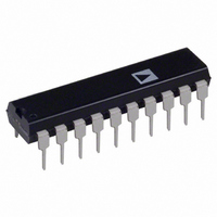
IC DAC 8BIT OCTAL CMOS 20-DIP
Manufacturer
Analog Devices Inc
Series
TrimDAC®r
Specifications of DAC8800FPZ
Data Interface
Serial
Settling Time
2µs
Number Of Bits
8
Number Of Converters
8
Voltage Supply Source
Dual ±
Power Dissipation (max)
12mW
Operating Temperature
-40°C ~ 85°C
Mounting Type
Through Hole
Package / Case
20-DIP (0.300", 7.62mm)
Resolution (bits)
8bit
Sampling Rate
1.25MSPS
Input Channel Type
Serial
Supply Current
1mA
Digital Ic Case Style
DIP
No. Of Pins
20
Lead Free Status / RoHS Status
Lead free / RoHS Compliant


PIN CONFIGURATIONS AND FUNCTION DESCRIPTIONS
PIN CONFIGURATIONS (N, R, RU, AND RW PACKAGES)
PIN CONFIGURATIONS (RS AND RU PACKAGES)
Table 3. Pin Function Descriptions
Mnemonic
V
V+
V–
GND
C1+, C1–
C2+, C2–
Tx
Tx
Rx
Rx
EN
SD
SD
DD
NC
CC
IN
OUT
IN
OUT
Figure 4. N, R, RU, and RW Packages Pin Configuration
Figure 6. RS and RU Packages Pin Configuration
Description
Internally Generated Positive Supply (+6 V nominal).
Ground Pin. Must be connected to 0 V.
are disabled.
No Connect.
Power Supply Input (3.3 V ± 0.3 V).
Internally Generated Negative Supply (−6 V nominal).
External Capacitor 1 is connected between these pins. A 0.1 μF capacitor is recommended but larger capacitors up to 47 μF
can be used.
External Capacitor 2 is connected between these pins. A 0.1 μF capacitor is recommended but larger capacitors up to 47 μF
can be used.
Transmitter (Driver) Inputs. These inputs accept TTL/CMOS levels.
Transmitter (Driver) Outputs. These are RS-232 signal levels (typically ±9 V).
Receiver Inputs. These inputs accept RS-232 signal levels. An internal 5 kΩ pull-down resistor to GND is connected on each input.
Receiver Outputs. These are CMOS output logic levels.
(ADM3222 only) Receiver Enable. Active low. When low, the receiver outputs are enabled. When high, they are three-stated.
(ADM3222 only) Shutdown Control. Active low. When low, the charge pump is shut down and the transmitter outputs
(ADM1385 only) Shutdown Control. When low, the charge pump is shut down and all transmitters and receivers are disabled.
(ADM1385 only) Driver Disable. When low, the charge pump is turned off and the transmitters are disabled. The receivers
remain active.
T2
R2
T2
R2
C1+
C1–
C2+
C2–
OUT
R2
C1+
C1–
C2+
C2–
OUT
OUT
V+
V–
EN
IN
V+
V–
IN
10
1
2
3
4
5
6
7
8
1
2
3
4
5
6
7
8
9
NC = NO CONNECT
(SSOP/TSSOP)
(Not to Scale)
(Not to Scale)
ADM3222
ADM3202
TOP VIEW
TOP VIEW
20
19
18
17
16
15
14
13
12
11
16
15
14
13
12
11
10
9
SD
V
GND
T1
R1
R1
NC
T1
T2
NC
V
GND
T1
R1
R1
T1
T2
R2
CC
CC
OUT
IN
IN
IN
OUT
OUT
IN
IN
IN
OUT
OUT
Rev. E | Page 5 of 16
Figure 5. N and RW Packages Pin Configuration
T2
Figure 7. RS Package Pin Configuration
T2
ADM3202/ADM3222/ADM1385
R2
R2
C1+
C1–
C2+
C2–
OUT
C1+
C1–
C2+
C2–
OUT
DD
NC
V+
V–
EN
V+
V–
IN
IN
10
1
2
3
4
5
6
7
8
9
1
2
3
4
5
6
7
8
9
NC = NO CONNECT
(Not to Scale)
(Not to Scale)
ADM3222
ADM1385
TOP VIEW
TOP VIEW
(SSOP)
18
17
16
15
14
13
12
11
10
20
19
18
17
16
15
14
13
12
11
SD
V
GND
T1
R1
R1
T1
T2
R2
SD
V
GND
T1
R1
R1
T1
T2
R2
NC
CC
CC
OUT
IN
IN
IN
OUT
OUT
OUT
IN
IN
IN
OUT
OUT
Related parts for DAC8800FPZ
Image
Part Number
Description
Manufacturer
Datasheet
Request
R

Part Number:
Description:
Analog Standard Cell 8-Bit Digital to Analog Converter
Manufacturer:
AMSCO [austriamicrosystems AG]
Datasheet:

Part Number:
Description:
±1.7g Dual-Axis IMEMS Accelerometer Evaluation Board
Manufacturer:
Analog Devices Inc
Datasheet:

Part Number:
Description:
Inertial Sensor Evaluation System
Manufacturer:
Analog Devices Inc
Datasheet:
Part Number:
Description:
Manufacturer:
Analog Devices Inc
Datasheet:
Part Number:
Description:
Manufacturer:
Analog Devices Inc
Datasheet:
Part Number:
Description:
Manufacturer:
Analog Devices Inc
Datasheet:
Part Number:
Description:
Manufacturer:
Analog Devices Inc
Datasheet:
Part Number:
Description:
Manufacturer:
Analog Devices Inc
Datasheet:
Part Number:
Description:
Manufacturer:
Analog Devices Inc
Datasheet:
Part Number:
Description:
Manufacturer:
Analog Devices Inc
Datasheet:
Part Number:
Description:
Manufacturer:
Analog Devices Inc
Datasheet:
Part Number:
Description:
Manufacturer:
Analog Devices Inc
Datasheet:
Part Number:
Description:
Manufacturer:
Analog Devices Inc
Datasheet: