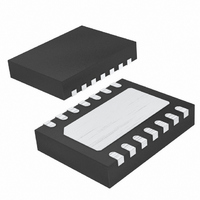
LTC2636IDE-HMX12#PBF Linear Technology, LTC2636IDE-HMX12#PBF Datasheet - Page 20

LTC2636IDE-HMX12#PBF
Manufacturer Part Number
LTC2636IDE-HMX12#PBF
Description
IC DAC 12-BIT OCTAL 14-DFN
Manufacturer
Linear Technology
Datasheet
1.LTC2636IDE-HMI12PBF.pdf
(24 pages)
Specifications of LTC2636IDE-HMX12#PBF
Settling Time
4.4µs
Number Of Bits
12
Data Interface
MICROWIRE™, Serial, SPI™
Number Of Converters
8
Voltage Supply Source
Single Supply
Power Dissipation (max)
2.7mW
Operating Temperature
-40°C ~ 85°C
Mounting Type
Surface Mount
Package / Case
14-DFN
Lead Free Status / RoHS Status
Lead free / RoHS Compliant
Available stocks
Company
Part Number
Manufacturer
Quantity
Price
OPERATION
LTC2636
at the REF pin. Adding bypass capacitance to the REF pin
will improve noise performance; and up to 10μF can be
driven without oscillation. The REF output must be buffered
when driving an external DC load current.
Alternatively, the DAC can operate in External Reference
mode using command 0111b. In this mode, an input voltage
supplied externally to the REF pin provides the reference
(1V ≤ V
external reference voltage supplied sets the full-scale DAC
output voltage. External Reference mode is the power-on
default for LTC2636-HMX/-LMX.
The reference mode of LTC2636-HZ/-LZ/-HMI/-LMI (Internal
Reference power-on default), can be changed by software
command after power-up. The same is true for LTC2636-
HMX/-LMX (External Reference power-on default).
Power-Down Mode
For power-constrained applications, power-down mode can
be used to reduce the supply current whenever less than
eight DAC outputs are needed. When in power-down, the
buffer amplifi ers, bias circuits, and integrated reference
circuits are disabled, and draw essentially zero current.
The DAC outputs are put into a high-impedance state, and
the output pins are passively pulled to ground through
individual 200k resistors. Input- and DAC-register contents
are not disturbed during power-down.
Any DAC channel or combination of channels can be put
into power-down mode by using command 0100b in
combination with the appropriate DAC address, (n). The
supply current is reduced approximately 10% for each DAC
powered down. The integrated reference is automatically
powered down when external reference is selected using
command 0111b. In addition, all the DAC channels and
the integrated reference together can be put into power-
down mode using Power Down Chip command 0101b.
When the integrated reference and all DAC channels are in
power-down mode, the REF pin becomes high impedance
(typically > 1GΩ). For all power-down commands the 16-
bit data word is ignored.
Normal operation resumes after executing any command
that includes a DAC update, (as shown in Table 1) or using
the asynchronous LDAC pin. The selected DAC is powered
20
REF
≤ V
CC
) and the supply current is reduced. The
up as its voltage output is updated. When a DAC which
is in a powered-down state is powered up and updated,
normal settling is delayed. If less than eight DACs are in
a powered-down state prior to the update command, the
power-up delay time is 10μs. However, if all eight DACs
and the integrated reference are powered down, then the
main bias generation circuit block has been automatically
shut down in addition to the DAC amplifi ers and reference
buffers. In this case, the power up delay time is 12μs.
The power-up of the integrated reference depends on
the command that powered it down. If the reference
is powered down using the Select External Reference
Command (0111b), then it can only be powered back
up using Select Internal Reference Command (0110b).
However, if the reference was powered down using Power
Down Chip Command (0101b), then in addition to Select
Internal Reference Command (0110b), any command (in
software or using the LDAC pin) that powers up the DACs
will also power up the integrated reference.
Voltage Outputs
The LTC2636’s integrated rail-to-rail amplifi ers have guar-
anteed load regulation when sourcing or sinking up to
10mA at 5V, and 5mA at 3V.
Load regulation is a measure of the amplifi er’s ability to
maintain the rated voltage accuracy over a wide range of
load current. The measured change in output voltage per
change in forced load current is expressed in LSB/mA.
DC output impedance is equivalent to load regulation, and
may be derived from it by simply calculating a change in
units from LSB/mA to ohms. The amplifi er’s DC output
impedance is 0.1Ω when driving a load well away from
the rails.
When drawing a load current from either rail, the output
voltage headroom with respect to that rail is limited by
the 50Ω typical channel resistance of the output devices
(e.g., when sinking 1mA, the minimum output voltage is
50Ω • 1mA, or 50mV). See the graph “Headroom at Rails
vs. Output Current” in the Typical Performance Charac-
teristics section.
The amplifi er is stable driving capacitive loads of up to
500pF .
2636fb


