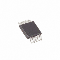
MAX5142EUB+ Maxim Integrated Products, MAX5142EUB+ Datasheet - Page 9

MAX5142EUB+
Manufacturer Part Number
MAX5142EUB+
Description
IC DAC 14BIT SER/VOLT I/O 10UMAX
Manufacturer
Maxim Integrated Products
Datasheet
1.MAX5143EUA.pdf
(12 pages)
Specifications of MAX5142EUB+
Settling Time
1µs
Number Of Bits
14
Data Interface
MICROWIRE™, QSPI™, Serial, SPI™
Number Of Converters
1
Voltage Supply Source
Single Supply
Power Dissipation (max)
444mW
Operating Temperature
-40°C ~ 85°C
Mounting Type
Surface Mount
Package / Case
10-MSOP, Micro10™, 10-uMAX, 10-uSOP
Resolution
14 bit
Interface Type
Serial (SPI)
Supply Voltage (max)
5.5 V
Supply Voltage (min)
4.5 V
Maximum Operating Temperature
+ 85 C
Mounting Style
SMD/SMT
Minimum Operating Temperature
- 40 C
Supply Current
0.2 mA
Voltage Reference
External
Lead Free Status / RoHS Status
Lead free / RoHS Compliant
cal at lower frequencies. The circuit can benefit from
even larger bypassing capacitors, depending on the
stability of the external reference with capacitive load-
ing.
Unbuffered operation reduces power consumption as
well as offset error contributed by the external output
buffer. The R-2R DAC output is available directly at
OUT, allowing 14-bit performance from +V
without degradation at zero scale. The DAC’s output
impedance is also low enough to drive medium loads
(R
the gain error is increased by externally loading the
DAC output.
The requirements on the external output buffer amplifier
change whether the DAC is used in unipolar or bipolar
operational mode. In unipolar mode, the output amplifi-
er is used in a voltage-follower connection. In bipolar
mode (MAX5142/MAX5144 only), the amplifier operates
with the internal scaling resistors (Figure 2b). In each
mode, the DAC’s output resistance is constant and is
independent of input code; however, the output amplifi-
er’s input impedance should still be as high as possible
to minimize gain errors. The DAC’s output capacitance
is also independent of input code, thus simplifying sta-
bility requirements on the external amplifier.
In bipolar mode, a precision amplifier operating with
dual power supplies (such as the MAX400) provides
the ±V
precision amplifiers with input common-mode ranges
including GND are available; however, their output
swings do not normally include the negative rail (GND)
without significant degradation of performance. A sin-
gle-supply op amp, such as the MAX495, is suitable if
the application does not use codes near zero.
Since the LSBs for a 14-bit DAC are extremely small
(152.6µV for V
external amplifier’s input specification. The input offset
voltage can degrade the zero-scale error and might
require an output offset trim to maintain full accuracy if
the offset voltage is greater than 1/2LSB. Similarly, the
input bias current multiplied by the DAC output resis-
tance (typically 6.25kΩ) contributes to zero-scale error.
Temperature effects also must be taken into considera-
tion. Over the -40°C to +85°C extended temperature
range, the offset voltage temperature coefficient (refer-
enced to +25°C) must be less than 0.95µV/°C to add
less than 1/2LSB of zero-scale error. The external
amplifier’s input resistance forms a resistive divider with
L
> 60kΩ) without degradation of INL or DNL; only
REF
output range. In single-supply applications,
External Output Buffer Amplifier
REF
_______________________________________________________________________________________
= +2.5V), pay close attention to the
Unbuffered Operation
REF
Voltage-Output, 14-Bit DACs
to GND
the DAC output resistance, which results in a gain error.
To contribute less than 1/2LSB of gain error, the input
resistance typically must be greater than:
The settling time is affected by the buffer input capaci-
tance, the DAC’s output capacitance, and PC board
capacitance. The typical DAC output voltage settling
time is 1µs for a full-scale step. Settling time can be sig-
nificantly less for smaller step changes. Assuming a
single time-constant exponential settling response, a
full-scale step takes 10.4 time constants to settle to
within 1/2LSB of the final output voltage. The time con-
stant is equal to the DAC output resistance multiplied
by the total output capacitance. The DAC output
capacitance is typically 10pF. Any additional output
capacitance increases the settling time.
The external buffer amplifier’s gain-bandwidth product
is important because it increases the settling time by
adding another time constant to the output response.
The effective time constant of two cascaded systems,
each with a single time-constant response, is approxi-
mately the root square sum of the two time constants.
The DAC output’s time constant is 1µs / 10.4 = 96ns,
ignoring the effect of additional capacitance. If the time
constant of an external amplifier with 1MHz bandwidth
is 1 / 2π (1MHz) = 159ns, then the effective time con-
stant of the combined system is:
This suggests that the settling time to within 1/2LSB of
the final output voltage, including the external buffer
amplifier, will be approximately 10.4
The digital interface for the 14-bit DAC is based on a
3-wire standard that is compatible with SPI, QSPI, and
MICROWIRE interfaces. The three digital inputs (CS,
DIN, and SCLK) load the digital input data serially into
the DAC.
A 20ns (min) logic low pulse to CLR clears the data in
the DAC buffer.
All of the digital inputs include Schmitt-trigger buffers to
accept slow-transition interfaces. This means that opto-
couplers can interface directly to the MAX5141–
MAX5144 without additional external logic. The digital
inputs are compatible with TTL/CMOS-logic levels.
+3V/+5V, Serial-Input,
Digital Inputs and Interface Logic
(
96ns
6.25k
)
2
Ω
+
×
(
159ns
2
15
)
=
2
205
=
186ns
✕
M
186ns = 1.93µs.
Ω
9


