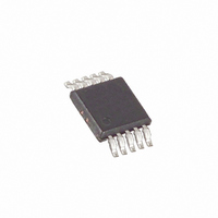
MAX5742AUB+ Maxim Integrated Products, MAX5742AUB+ Datasheet - Page 3

MAX5742AUB+
Manufacturer Part Number
MAX5742AUB+
Description
IC DAC 12BIT QUAD LP SER 10-UMAX
Manufacturer
Maxim Integrated Products
Datasheet
1.MAX5742EUB.pdf
(15 pages)
Specifications of MAX5742AUB+
Settling Time
4µs
Number Of Bits
12
Data Interface
Serial
Number Of Converters
4
Voltage Supply Source
Single Supply
Operating Temperature
-40°C ~ 125°C
Mounting Type
Surface Mount
Package / Case
10-MSOP, Micro10™, 10-uMAX, 10-uSOP
Number Of Dac Outputs
4
Resolution
12 bit
Interface Type
Serial (SPI)
Supply Voltage (max)
5.5 V
Supply Voltage (min)
2.7 V
Maximum Operating Temperature
+ 125 C
Mounting Style
SMD/SMT
Minimum Operating Temperature
- 40 C
Supply Current
420 uA
Voltage Reference
External
Lead Free Status / RoHS Status
Lead free / RoHS Compliant
Power Dissipation (max)
-
Lead Free Status / Rohs Status
Lead free / RoHS Compliant
ELECTRICAL CHARACTERISTICS (continued)
(V
V
TIMING CHARACTERISTICS
(V
Note 1: DC specifications are tested without output loads.
Note 2: Linearity guaranteed from code 115 to code 3981.
Note 3: Limited with test conditions.
Note 4: Offset and gain error limit the FSR.
Note 5: Guaranteed by design.
DD
Input High Voltage
Input Low Voltage
Input Leakage Current
Input Capacitance
DYNAMIC PERFORMANCE
Voltage Output Slew Rate
Voltage Output Settling Time
Digital Feedthrough
Digital-Analog Glitch Impulse
DAC-to-DAC Crosstalk
POWER REQUIREMENTS
Supply-Voltage Range
Supply Current with No Load
Power-Down Supply Current
SCLK Clock Frequency
SCLK Pulse Width High
SCLK Pulse Width Low
CS Fall to SCLK Rise Setup Time
SCLK Fall to CS Rise Setup Time
DIN to SCLK Fall Setup Time
DIN to SCLK Fall Hold Time
CS Pulse Width High
DIGITAL INPUTS (SCLK, DIN, CS)
DD
DD
= +5V, T
= 2.7V to 5.5V, GND = 0, T
= +2.7V to +5.5V, GND = 0, V
PARAMETER
PARAMETER
A
= +25°C.)
12-Bit, Low-Power, Quad, Voltage-Output
_______________________________________________________________________________________
A
= T
REF
SYMBOL
MIN
SYMBOL
I
DDPD
= V
V
f
C
V
I
V
SR
t
I
t
t
DD
SCLK
CSW
IN
DD
t
t
t
CSS
CSH
t
IH
IL
IN
to T
CH
DH
CL
DS
DD
MAX
, R
L
V
V
Digital inputs = 0 or V
400 hex to C00 hex (Note 5)
Any digital inputs from 0 to V
Major carry transition (code 7FF hex to code
800 hex)
All digital inputs at 0 or V
All digital inputs at 0 or V
All digital inputs at 0 or V
, unless otherwise noted.)
= 5k , C
DD
DD
= +3V, +5V
= +3V, +5V
L
= 200pF, T
DAC with Serial Interface
CONDITIONS
CONDITIONS
DD
A
= T
DD
DD
DD
MIN
= 3.6V
= 5.5V
= 5.5V
DD
to T
MAX
, unless otherwise noted. Typical values are
0.7 x
V
MIN
MIN
2.7
25
25
10
10
15
80
DD
0
0
TYP
0.29
TYP
229
271
0.5
0.1
2.4
12
0.1
5
4
MAX
0.3 x
MAX
V
395
420
5.5
10
20
DD
1
1
UNITS
UNITS
nV-s
nV-s
nV-s
MHz
V/µs
µA
pF
µA
µA
µs
ns
ns
ns
ns
ns
ns
ns
V
V
V
3


