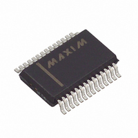
MAX5322EAI+ Maxim Integrated Products, MAX5322EAI+ Datasheet - Page 14

MAX5322EAI+
Manufacturer Part Number
MAX5322EAI+
Description
IC DAC 12BIT DUAL 10V SER 28SSOP
Manufacturer
Maxim Integrated Products
Datasheet
1.MAX5322EAI.pdf
(18 pages)
Specifications of MAX5322EAI+
Settling Time
10µs
Number Of Bits
12
Data Interface
Serial
Number Of Converters
2
Voltage Supply Source
Analog and Digital, Dual ±
Operating Temperature
-40°C ~ 85°C
Mounting Type
Surface Mount
Package / Case
28-SSOP
Resolution
12 bit
Interface Type
Serial (SPI)
Supply Voltage (max)
15.75 V
Supply Voltage (min)
10.8 V
Maximum Operating Temperature
+ 85 C
Mounting Style
SMD/SMT
Minimum Operating Temperature
- 40 C
Voltage Reference
External
Lead Free Status / RoHS Status
Lead free / RoHS Compliant
Power Dissipation (max)
-
Lead Free Status / Rohs Status
Lead free / RoHS Compliant
and isolate the shift register from the DAC registers.
The DAC registers control the DAC ladder and thus the
output voltage. Any update to a DAC register updates
the respective output voltage.
Data in the shift register is transferred to the input regis-
ters during the appropriate software command only.
Data in the input registers is transferred to the DAC
registers in two ways: using the software command, or
through external logic control using the asynchronous
load input (LDAC). Table 2 shows the software com-
mands that transfer the data from the shift register to
the input and/or DAC registers. The CLR, an external
logic control, asynchronously forces all outputs to 0V, in
both unipolar and bipolar modes. Interface timing is
shown in Figures 2 and 3.
Wait a minimum of 100ns after CS goes high before
implementing LDAC or CLR. If either of these logic
inputs activates during a data transfer, the incoming
data is corrupted and needs to be reloaded. For soft-
ware control only, tie LDAC and CLR high.
±10V, Dual, 12-Bit, Serial, Voltage-Output DAC
Figure 2. Serial-Interface Signals
Figure 3. Serial-Interface Timing Diagram
14
______________________________________________________________________________________
DOUT
LDAC
SCLK
DIN
CS
SCLK
DIN
CS
t
CS0
C3
1
t
C2
CSE
t
CSS
t
DS
C1
MSB
C0
t
DH
D11
t
CH
D10
t
CP
D9
t
DO1
t
D8
CL
8
D7
LSB
9
The MAX5322 uses an inverted DAC ladder architec-
ture to convert the digital input into an analog output
voltage. The digital input controls weighted switches
that connect the DAC-ladder nodes to either REFA
(REFB) or GND (Figure 4). The sum of the weights pro-
duces the analog equivalent of the digital-input word
and is then buffered at the output.
Connect an external reference of 2V to 5.25V to REFA
and REFB. Set the output voltage range with the refer-
ence and the input code by using the equations below.
Unipolar output voltage:
D6
D5
D4
t
CSH
V
External Reference and Transfer
OUT UNI
D3
_
COMMAND EXECUTED
D2
=
t
CS1
LSB
D1
t
CSD
t
LDS
UNI
D0
16
DAC Architecture
t
×
CSW
CODE
t
LD
(1)
Functions


