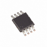
MAX5352BEUA+ Maxim Integrated Products, MAX5352BEUA+ Datasheet - Page 3

MAX5352BEUA+
Manufacturer Part Number
MAX5352BEUA+
Description
IC DAC 12BIT VOLT OUT SER 8-UMAX
Manufacturer
Maxim Integrated Products
Datasheet
1.MAX5352BCPA.pdf
(16 pages)
Specifications of MAX5352BEUA+
Settling Time
14µs
Number Of Bits
12
Data Interface
Serial
Number Of Converters
1
Voltage Supply Source
Single Supply
Power Dissipation (max)
330mW
Operating Temperature
-40°C ~ 85°C
Mounting Type
Surface Mount
Package / Case
8-MSOP, Micro8™, 8-uMAX, 8-uSOP,
Number Of Dac Outputs
1
Resolution
12 bit
Interface Type
Serial (SPI)
Supply Voltage (max)
5.5 V
Supply Voltage (min)
4.5 V
Maximum Operating Temperature
+ 85 C
Mounting Style
SMD/SMT
Minimum Operating Temperature
- 40 C
Supply Current
400 uA
Voltage Reference
External
Lead Free Status / RoHS Status
Lead free / RoHS Compliant
ELECTRICAL CHARACTERISTICS: MAX5352 (continued)
(V
T
Note 1: Guaranteed from code 11 to code 4095 in unity-gain configuration.
Note 2: Accuracy is better than 1LSB for V
Note 3: R
DIGITAL INPUTS
DYNAMIC PERFORMANCE
Voltage Output Slew Rate
Output Settling Time
Output Voltage Swing
Current into FB
Start-Up Time
Digital Feedthrough
POWER SUPPLIES
Supply Voltage
Supply Current
Supply Current in Shutdown
Reference Current in Shutdown
SCLK Clock Period
SCLK Pulse Width High
SCLK Pulse Width Low
CS Fall to SCLK Rise Setup Time
SCLK Rise to CS Rise Hold Time
DIN Setup Time
DIN Hold Time
SCLK Rise to CS Fall Delay
CS Rise to SCLK Rise Hold Time
CS Pulse Width High
A
TIMING CHARACTERISTICS (Figure 6)
DD
= +25°C. Output buffer connected in unity-gain configuration (Figure 8).)
= +5V ±10%, REF = 2.5V, GND = 0V, R
end points.
PARAMETER
L
= , digital inputs at GND or V
_______________________________________________________________________________________
Low-Power, 12-Bit Voltage-Output DACs
SYMBOL
t
t
t
t
t
V
CSW
I
t
CSH
t
t
t
CSS
t
CS0
CS1
SR
DD
CH
DH
CP
CL
DS
DD
DD
OUT
L
.
To ±1/2LSB, V
Rail-to-rail (Note 2)
CS = V
(Note 3)
(Note 3)
= 5kΩ, C
= 8mV to V
DD
L
, DIN = 100kHz
= 100pF, T
DD
STEP
- 100mV, guaranteed by a power-supply rejection test at the
CONDITIONS
= 2.5V
A
= T
MIN
with Serial Interface
to T
MAX
, unless otherwise noted. Typical values are at
MIN
100
100
4.5
40
40
40
40
40
40
0
0
0 to V
0.001
0.001
TYP
0.28
0.6
14
20
5
4
DD
MAX
±0.1
±0.5
5.5
0.4
20
UNITS
V/µs
nV-s
mA
µA
µA
µA
µs
µs
ns
ns
ns
ns
ns
ns
ns
ns
ns
ns
V
V
3


