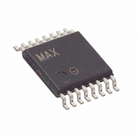
MAX5308EUE+ Maxim Integrated Products, MAX5308EUE+ Datasheet - Page 11

MAX5308EUE+
Manufacturer Part Number
MAX5308EUE+
Description
IC DAC 10BIT OCT LP SER 16-TSSOP
Manufacturer
Maxim Integrated Products
Datasheet
1.MAX5308EUE.pdf
(15 pages)
Specifications of MAX5308EUE+
Settling Time
5µs
Number Of Bits
10
Data Interface
Serial
Number Of Converters
8
Voltage Supply Source
Single Supply
Power Dissipation (max)
775mW
Operating Temperature
-40°C ~ 85°C
Mounting Type
Surface Mount
Package / Case
16-TSSOP
Resolution
12 bit
Interface Type
Serial (SPI)
Supply Voltage (max)
5.5 V
Supply Voltage (min)
2.7 V
Maximum Operating Temperature
+ 85 C
Mounting Style
SMD/SMT
Minimum Operating Temperature
- 40 C
Supply Current
1.7 mA
Voltage Reference
External
Lead Free Status / RoHS Status
Lead free / RoHS Compliant
Figure 2. Connections for MICROWIRE
and terminate all DAC outputs to GND through 100kΩ
resistors. CLR is asynchronous and can be applied at
any time. If CLR is toggled low during loading of a seri-
al word, that word will terminate and must be reloaded.
The external reference input has a typical input imped-
ance of 200kΩ. The input voltage range is from 800mV
to V
MAX5308/MAX5309. The DAC outputs are then ratio-
metric to V
The rail-to-rail buffer amplifier is stable with any combi-
nation of resistive loads greater than 2kΩ and capaci-
tive loads less than 500pF. With a capacitive load of
200pF the output buffers have a slew rate of 1V/µs. For
a 1/4 FS to 3/4 FS output transition, the amplifier output
typically settles to 1/2 LSB in less than 10µs when
loaded with 2kΩ in parallel with 200pF.
The MAX5308/MAX5309 have a POR circuit to set the
DACs’ output to zero when V
ensures that unwanted DAC output voltages will not
occur immediately following a system startup, such as
after a loss of power. Upon initial power-up the POR cir-
cuit ensures that all DAC registers are cleared, the
DACs are powered-down, and their outputs are termi-
nated to GND through a 100kΩ resistor.
*THE DOUT-SI CONNECTION IS NOT REQUIRED FOR WRITING TO THE MAX5308,
BUT MAY BE USED FOR TRANSMISSION VERIFICATION PURPOSES.
DD
Low-Power, Low-Glitch, Octal 10-Bit Voltage-
. V
MAX5308
DD
DD
.
can be used as the reference for the
DOUT*
SCLK
______________________________________________________________________________________
DIN
CS
DD
Output DACs with Serial Interface
SK
SO
SI*
I/O
Reference Input
Power-On Reset
is first applied. This
Output Buffer
MICROWIRE
PORT
Any number of MAX5308s can be daisy-chained by
connecting the DOUT pin of one device to the DIN pin
of the following device in the chain (Figure 5). To write
to the chain, drive CS low until all n
(where n is the number of devices in the chain) and
associated data have been applied to the first device.
When CS is driven high, each device in the chain acts
on the 16 bits in its input register. To adjust a single
device in the chain, a No-Operation (NOP) command
must be loaded for all other devices.
Figure 6 shows an alternate method of connecting sev-
eral MAX5308s or MAX5309s. In this configuration, the
data bus is common to all devices; data is not shifted
through a daisy chain. More I/O lines are required in
this configuration because a dedicated chip-select
input (CS) is required for each IC.
The MAX5308/MAX5309 are normally configured for
unipolar output. Table 3 lists the unipolar output volt-
ages vs. digital codes.
The MAX5308/MAX5309 outputs can be configured for
bipolar operation using Figure 7’s circuit.
Figure 3. Connections for SPI/QSPI
*THE DOUT-MISO CONNECTION IS NOT REQUIRED FOR WRITING TO THE MAX5309,
BUT MAY BE USED FOR TRANSMISSION VERIFICATION PURPOSES.
MAX5308
V
OUT
DOUT*
Applications Information
SCLK
DIN
CS
= V
REF
Daisy-Chaining Devices
[(2D / 1024) -1]
CPOL = 0, CPHA = 0
MISO*
MOSI
SCK
I/O
Unipolar Output
Bipolar Output
✕
SPI/QSPI
16 clock cycles
PORT
+5V
SS
11


