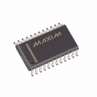
MAX530BCWG+ Maxim Integrated Products, MAX530BCWG+ Datasheet

MAX530BCWG+
Specifications of MAX530BCWG+
Related parts for MAX530BCWG+
MAX530BCWG+ Summary of contents
Page 1
... D0/D8 D4 D2/D10 D6 D1/D9 D3/D11 D5 D7 ________________________________________________________________ Maxim Integrated Products Call toll free 1-800-998-8800 for free samples or literature. +5V, Low-Power, Parallel-Input, Voltage-Output, 12-Bit DAC ____________________________Features Buffered Voltage Output Internal 2.048V Voltage Reference Operates from Single +5V or Dual ±5V Supplies Low Power Consumption: 250µA Operating Current 40µ ...
Page 2
Low-Power, Parallel-Input, Voltage-Output, 12-Bit DAC ABSOLUTE MAXIMUM RATINGS V to DGND and V to AGND ................................-0.3V, + DGND and V to AGND .................................-6V, +0. ............................................................... -0.3V, +12V DD SS AGND ...
Page 3
ELECTRICAL CHARACTERISTICS—Single +5V Supply (continued ±10 0V, AGND = DGND = REFGND = 0V, REFIN = 2.048V (external), RFB = ROFS = VOUT 10kΩ 100pF ...
Page 4
Low-Power, Parallel-Input, Voltage-Output, 12-Bit DAC ELECTRICAL CHARACTERISTICS—Dual ±5V Supplies ( ±10 -5V ±10%, AGND = DGND = REFGND = 0V, REFIN = 2.048V (external), RFB = ROFS = VOUT 33µF, R ...
Page 5
ELECTRICAL CHARACTERISTICS—Dual ±5V Supplies (continued ±10 -5V ±10%, AGND = DGND = REFGND = 0V, REFIN = 2.048V (external), RFB = ROFS = VOUT 33µ 10kΩ 100pF, ...
Page 6
Low-Power, Parallel-Input, Voltage-Output, 12-Bit DAC ____________________________Typical Operating Characteristics (continued +25°C, single supply (+5V), unity gain, code = all 1s, unless otherwise noted). A SUPPLY CURRENT vs. TEMPERATURE 300 290 280 270 260 250 240 230 60 100 ...
Page 7
Description PIN NAME 1 D1 Input Dta, when and Input when D2/ D10 D2 Input Dta, when and A1 = ...
Page 8
Low-Power, Parallel-Input, Voltage-Output, 12-Bit DAC ________________Detailed Description The MAX530 consists of a parallel-input logic interface, a 12-bit R-2R ladder, a reference, and an op amp. The Functional Diagram shows the control lines and signal flow through the input data ...
Page 9
R REFOUT S TOTAL C S REFERERNCE NOISE C REFOUT TEK 7A22 300 SINGLE POLE ROLLOFF 250 C = 3.3 F REFOUT 200 150 100 50 C REFOUT 0 0 100 FREQUENCY (kHz) Figure 2. Reference Noise vs. ...
Page 10
Low-Power, Parallel-Input, Voltage-Output, 12-Bit DAC 33 F REFGND 2N7002 AGND DGND CLR LDAC Figure 3. Low-Current Shutdown Mode An additional 110µA of supply current can be saved when the internal reference is not used by ...
Page 11
A0- DATA BITS (8-BIT BYTE OR 4-BIT NIBBLE) CLR t CLR LDAC NOTE: TIMING MEASUREMENT REFERENCE LEVEL IS Figure 4. MAX530 Write-Cycle Timing Diagram Parallel Logic Interface Designed to interface with 4-bit, 8-bit, and 16-bit micro- processors (µPs), ...
Page 12
Low-Power, Parallel-Input, Voltage-Output, 12-Bit DAC D0-D3 DATA BUS D0-D3 FROM D0-D3 SYSTEM CLR RESET A0, A1 MC6800 DECODER R/W ADDRESS BUS A0, A1 A0-A15 A13-A15 Figure 5. 4-Bit µP Interface ...
Page 13
NBL & NBM NBH CS WR LDAC = 0 (DAC LATCH IS TRANSPARENT) Figure 8b. 8-Bit and 16-Bit µP Timing Sequence with LDAC = 0 Unipolar Configuration The MAX530 is configured for +2.048V unipolar output range by ...
Page 14
Low-Power, Parallel-Input, Voltage-Output, 12-Bit DAC Table 3. Unipolar Binary Code Table ( Output), Gain = 1 REFIN OUTPUT INPUT 1111 1111 1111 (V REFIN 1000 0000 0001 (V REFIN 2048 1000 0000 (V ) 0000 REFIN 4096 ...
Page 15
REFIN ROFS REFOUT 33µF MAX530 RFB AGND DGND VOUT REFGND -5V Figure 11. Bipolar Configuration (-2.048V to +2.048V Output) __________Applications Information Single-Supply Linearity As with any amplifier, the MAX530’s output op amp offset can be positive or negative. When ...
Page 16
... Maxim cannot assume responsibility for use of any circuitry other than circuitry entirely embodied in a Maxim product. No circuit patent licenses are implied. Maxim reserves the right to change the circuitry and specifications without notice at any time. 16 __________________Maxim Integrated Products, 120 San Gabriel Drive, Sunnyvale, CA 94086 (408) 737-7600 © 1995 Maxim Integrated Products ...


