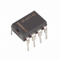
MAX5352BCPA+ Maxim Integrated Products, MAX5352BCPA+ Datasheet - Page 12

MAX5352BCPA+
Manufacturer Part Number
MAX5352BCPA+
Description
IC DAC V-OUT 12BIT 5V LP 8-DIP
Manufacturer
Maxim Integrated Products
Datasheet
1.MAX5352BCPA.pdf
(16 pages)
Specifications of MAX5352BCPA+
Settling Time
14µs
Number Of Bits
12
Data Interface
Serial
Number Of Converters
1
Voltage Supply Source
Single Supply
Power Dissipation (max)
727mW
Operating Temperature
0°C ~ 70°C
Mounting Type
Through Hole
Package / Case
8-DIP (0.300", 7.62mm)
Resolution
12 bit
Interface Type
Serial (3-Wire, SPI, QSPI, Microwire)
Supply Voltage (max)
5.5 V
Supply Voltage (min)
4.5 V
Maximum Operating Temperature
+ 70 C
Mounting Style
Through Hole
Minimum Operating Temperature
0 C
Lead Free Status / RoHS Status
Lead free / RoHS Compliant
Figure 7 shows a method of connecting several
MAX5352/MAX5353s. In this configuration, the clock
and the data bus are common to all devices, and sepa-
rate chip-select lines are used for each IC.
For a unipolar output, the output voltage and the refer-
ence input have the same polarity. Figure 8 shows the
MAX5352/MAX5353 unipolar output circuit, which is
also the typical operating circuit. Table 2 lists the unipo-
lar output codes.
Figure 9 illustrates a rail-to-rail output. This circuit
shows the MAX5352 with the output amplifier config-
ured with a closed-loop gain of +2 to provide a 0V to 5V
full-scale range when a 2.5V reference is used. When
the MAX5353 is used with a 1.25V reference, this circuit
provides a 0V to 2.5V full-scale range.
The MAX5352/MAX5353 output can be configured for
bipolar operation using Figure 10’s circuit according to
the following equation:
where NB is the numeric value of the DAC’s binary input
code. Table 3 shows digital codes (offset binary) and
the corresponding output voltage for Figure 10’s circuit.
Low-Power, 12-Bit Voltage-Output DACs
with Serial Interface
Figure 7. Multiple MAX5352/MAX5353s Sharing Common DIN and SCLK Lines
12
__________Applications Information
______________________________________________________________________________________
SCLK
CS1
CS2
CS3
DIN
V
OUT
= V
REF
CS
SCLK
DIN
[(2NB / 4096) - 1]
MAX5352
MAX5353
Unipolar Output
Bipolar Output
CS
SCLK
DIN
MAX5352
MAX5353
NOTE: ( ) are for sub-bit.
In applications where the reference has AC-signal com-
ponents, the MAX5352/MAX5353 have multiplying
capability within the reference input range specifica-
tions. Figure 11 shows a technique for applying a sine-
wave signal to the reference input where the AC signal
is offset before being applied to REF. The reference
voltage must never be more negative than GND.
Table 2. Unipolar Code Table
MSB
1 1 1 1 1 1 1 1 1 1 1 1 ( 0 )
1 0 0 0 0 0 0 0 0 0 0 1 ( 0 )
1 0 0 0 0 0 0 0 0 0 0 0 ( 0 )
0 1 1 1 1 1 1 1 1 1 1 1 ( 0 )
0 0 0 0 0 0 0 0 0 0 0 1 ( 0 )
0 0 0 0 0 0 0 0 0 0 0 0 ( 0 )
DAC CONTENTS
CS
SCLK
DIN
LSB
MAX5352
MAX5353
Using an AC Reference
+V
REF
ANALOG OUTPUT
+V
+V
+V
+V
2048
4096
REF
REF
REF
REF
TO OTHER
SERIAL DEVICES
0V
2049
4096
2047
4096
4096
4095
4096
1
V
REF
2


