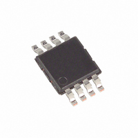
MAX5302CUA+ Maxim Integrated Products, MAX5302CUA+ Datasheet - Page 10

MAX5302CUA+
Manufacturer Part Number
MAX5302CUA+
Description
IC DAC 12BIT LP SERIAL 8-UMAX
Manufacturer
Maxim Integrated Products
Datasheet
1.MAX5302CUA.pdf
(12 pages)
Specifications of MAX5302CUA+
Settling Time
14µs
Number Of Bits
12
Data Interface
Serial
Number Of Converters
1
Voltage Supply Source
Single Supply
Operating Temperature
0°C ~ 70°C
Mounting Type
Surface Mount
Package / Case
8-MSOP, Micro8™, 8-uMAX, 8-uSOP,
Number Of Dac Outputs
1
Resolution
12 bit
Interface Type
Serial (SPI)
Supply Voltage (max)
5.5 V
Supply Voltage (min)
4.5 V
Maximum Operating Temperature
+ 70 C
Mounting Style
SMD/SMT
Minimum Operating Temperature
0 C
Supply Current
400 uA
Voltage Reference
External
Lead Free Status / RoHS Status
Lead free / RoHS Compliant
Power Dissipation (max)
-
Lead Free Status / Rohs Status
Lead free / RoHS Compliant
The circuit of Figure 12 places an NPN transistor (2N3904
or similar) within the op amp feedback loop to implement
a digitally programmable, unidirectional current source.
The output current is calculated with the following
equation:
where NB is the numeric value of the DAC’s binary input
code, and R is the sense resistor shown in Figure 12.
On power-up, the input and DAC registers are cleared
(set to zero code).
For rated MAX5302 performance, V
1.4V below V
parallel with a 0.1µF capacitor to GND. Use short lead
lengths and place the bypass capacitors as close to
the supply pins as possible.
Digital or AC transient signals on GND can create noise
at the analog output. Connect GND to the highest-quality
ground available.
Good PC board ground layout minimizes crosstalk
between the DAC output, reference input, and digital
input. Reduce crosstalk by keeping analog lines away
from digital lines. Wire-wrapped boards are not recom-
mended.
Low-Power, 12-Bit Voltage-Output DAC
with Serial Interface
Figure 9. Unipolar Rail-to-Rail Output Circuit
10
Digitally Programmable Current Source
______________________________________________________________________________________
Grounding and Layout Considerations
REF
I
DD
OUT
. Bypass V
DAC
MAX5302
Power-Supply Considerations
= (V
REF
/ R) (NB / 4096)
DD
+5V
V
DD
with a 4.7µF capacitor in
GND
REF
FB
OUT
must be at least
10k
10k
Figure 10. Bipolar Output Circuit
Table 3. Bipolar Code Table
Note: ( ) are for sub-bit.
MSB
1 1 1 1 1 1 1 1 11 1 1 ( 0 )
1 0 0 0 0 0 0 0 00 0 1 ( 0 )
1 0 0 0 0 0 0 0 00 0 0 ( 0 )
0 1 1 1 1 1 1 1 11 1 1 ( 0 )
0 0 0 0 0 0 0 0 00 0 1 ( 0 )
0 0 0 0 0 0 0 0 00 0 0 ( 0 )
REF
DAC CONTENTS
DAC
MAX5302
R1
GND
V
+5V
DD
LSB
OUT
FB
-V
ANALOG OUTPUT
REF
+V
+V
-V
-V
2048
2048
R1 = R2 = 10kΩ ±0.1%
REF
REF
V+
REF
REF
V-
R2
0V
=
2047
2048
2048
2048
2047
2048
1
1
- V
REF
V
OUT


