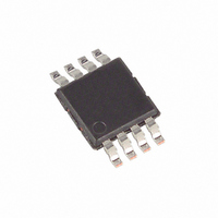
MAX5533EUA+ Maxim Integrated Products, MAX5533EUA+ Datasheet - Page 17

MAX5533EUA+
Manufacturer Part Number
MAX5533EUA+
Description
IC DAC 12BIT DUAL ULP 8-UMAX
Manufacturer
Maxim Integrated Products
Datasheet
1.MAX5532EUA.pdf
(24 pages)
Specifications of MAX5533EUA+
Settling Time
660µs
Number Of Bits
12
Data Interface
MICROWIRE™, QSPI™, Serial, SPI™
Number Of Converters
2
Voltage Supply Source
Single Supply
Power Dissipation (max)
471mW
Operating Temperature
-40°C ~ 85°C
Mounting Type
Surface Mount
Package / Case
8-MSOP, Micro8™, 8-uMAX, 8-uSOP,
Number Of Dac Outputs
2
Resolution
12 bit
Interface Type
Serial (SPI)
Supply Voltage (max)
5.5 V
Supply Voltage (min)
1.8 V
Maximum Operating Temperature
+ 85 C
Mounting Style
SMD/SMT
Minimum Operating Temperature
- 40 C
Supply Current
0.008 mA
Voltage Reference
Internal
Lead Free Status / RoHS Status
Lead free / RoHS Compliant
The MAX5532–MAX5535 feature two power modes to
conserve power during idle periods. In normal opera-
tion, the device is fully operational. In shutdown mode,
the device is completely powered down, including the
internal voltage reference in the MAX5533/MAX5535.
The MAX5533/MAX5535 also offer a standby mode in
which all circuitry is powered down except the internal
voltage reference. Standby mode keeps the reference
powered up while the remaining circuitry is shut down,
allowing it to be used as a system reference. It also
helps reduce the wake-up delay by not requiring the ref-
erence to power up when returning to normal operation.
The MAX5532–MAX5535 feature a software-program-
mable shutdown mode that reduces the supply current
and the reference input current to 0.18µA (max).
Writing an input control word with control bits C[3:0] =
1110 (Table 2) places the device in shutdown mode. In
shutdown, the MAX5532/MAX5534 reference input and
DAC output buffers go high impedance. Placing the
MAX5533/MAX5535 into shutdown turns off the internal
reference and the DAC output buffers go high imped-
ance. The serial interface still remains active for
all devices.
Table 2 shows several commands that bring the
MAX5532–MAX5535 back to normal operation. The
power-up time from shutdown is required before the
DAC outputs are valid.
Note: For the MAX5533/MAX5535, standby mode can-
not be entered directly from shutdown mode. The
device must be brought into normal operation first
before entering standby mode.
The MAX5533/MAX5535 feature a software-program-
mable standby mode that reduces the typical supply
current to 3µA (max). Standby mode powers down all
circuitry except the internal voltage reference. Place
the device in standby mode by writing an input control
word with control bits C[3:0] = 1100 (Table 2). The
internal reference and serial interface remain active
while the DAC output buffers go high impedance.
Standby Mode (MAX5533/MAX5535 Only)
______________________________________________________________________________________
Power Modes
Shutdown Mode
12-Bit, Voltage-Output DACs
For the MAX5533/MAX5535, standby mode cannot be
entered directly from shutdown mode. The device must
be brought into normal operation first before entering
standby mode. To enter standby from shutdown, issue
the command to return to normal operation followed
immediately by the command to go into standby.
Table 2 shows several commands that bring the
MAX5533/MAX5535 back to normal operation. When
transitioning from standby mode to normal operation,
only the DAC power-up time is required before the DAC
outputs are valid.
The MAX5532/MAX5534 accept a reference with a volt-
age range extending from 0 to V
(V
age source as:
where N is the numeric value of the DAC’s binary input
code (0 to 4095), V
the externally set voltage gain for the MAX5534, and
gain is one for the MAX5532.
In shutdown mode, the reference input enters a high-
impedance state with an input impedance of 2.5G (typ).
The MAX5533/MAX5535 internal voltage reference is soft-
ware configurable to one of four voltages. Upon power-
up, the default reference voltage is 1.214V. Configure the
reference voltage using D10 and D11 data bits (Table 3)
when the control bits are as follows C[3:0] = 1100, 1101,
or 1110 (Table 2). V
200mV above V
Table 3. Reference Output Voltage
Programming
Dual, Ultra-Low-Power,
OUT
D11
0
0
1
1
) is represented by a digitally programmable volt-
V
OUT
REF
D10
0
1
0
1
= (V
for proper operation.
REF
DD
REF
is the reference voltage, gain is
must be kept at a minimum of
x N / 4096) x gain
REFERENCE VOLTAGE (V)
DD
Reference Output
Reference Input
. The output voltage
1.214
1.940
2.425
3.885
17


