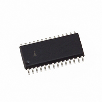
HI5731BIB Intersil, HI5731BIB Datasheet - Page 9

HI5731BIB
Manufacturer Part Number
HI5731BIB
Description
IC DAC 12-BIT 100MSPS 28-SOIC
Manufacturer
Intersil
Datasheet
1.HI5731BIB.pdf
(17 pages)
Specifications of HI5731BIB
Settling Time
20ns
Number Of Bits
12
Data Interface
Parallel
Number Of Converters
1
Voltage Supply Source
Analog and Digital, Dual ±
Power Dissipation (max)
650mW
Operating Temperature
-40°C ~ 85°C
Mounting Type
Surface Mount
Package / Case
28-SOIC (7.5mm Width)
Lead Free Status / RoHS Status
Contains lead / RoHS non-compliant
Available stocks
Company
Part Number
Manufacturer
Quantity
Price
Company:
Part Number:
HI5731BIB
Manufacturer:
HARRIS
Quantity:
37
Part Number:
HI5731BIB
Manufacturer:
H
Quantity:
20 000
Part Number:
HI5731BIBZ
Manufacturer:
INTERSIL
Quantity:
20 000
Pin Descriptions
Detailed Description
The HI5731 is a 12-bit, current out D/A converter. The DAC can
convert at 100MSPS and runs on +5V and -5.2V supplies. The
architecture is an R/2R and segmented switching current cell
arrangement to reduce glitch. Laser trimming is employed to
tune linearity to true 12-bit levels. The HI5731 achieves its low
power and high speed performance from an advanced
BiCMOS process. The HI5731 consumes 650mW (typical) and
has an improved hold time of only 0.25ns (typical). The HI5731
is an excellent converter for use in communications applications
and high performance instrumentation systems.
Digital Inputs
The HI5731 is a TTL/CMOS compatible D/A. Data is latched
by a Master register. Once latched, data inputs D0 (LSB)
thru D11 (MSB) are internally translated from TTL to ECL.
The internal latch and switching current source controls are
implemented in ECL technology to maintain high switching
speeds and low noise characteristics.
Decoder/Driver
The architecture employs a split R/2R ladder and
Segmented Current source arrangement. Bits D0 (LSB) thru
D7 directly drive a typical R/2R network to create the binary
weighted current sources. Bits D8 thru D11 (MSB) pass thru
a “thermometer” decoder that converts the incoming data
into 15 individual segmented current source enables. This
split architecture helps to improve glitch, thus resulting in a
more constant glitch characteristic across the entire output
transfer function.
Clocks and Termination
The internal 12-bit register is updated on the rising edge of
the clock. Since the HI5731 clock rate can run to 100MSPS,
PIN NUMBER
13, 14
17, 28
1-12
15
16
18
23
27
19
21
20
22
24
25
26
D11 (MSB) thru
CTRL OUT
PIN NAME
REF OUT
D0 (LSB)
CTRL IN
DGND
AGND
ARTN
DV
DV
R
AV
I
I
CLK
OUT
OUT
NC
SET
CC
EE
EE
9
Digital Data Bit 11, the Most Significant Bit thru Digital Data Bit 0, the Least Significant Bit.
Data Clock Pin DC to 100MSPS.
No Connect.
Digital Logic Supply +5V.
Digital Ground.
-5.2V Logic supply.
External resistor to set the full scale output current. I
Analog Ground supply current return pin.
Analog Signal Return for the R/2R ladder.
Current Output Pin.
Complementary Current Output Pin.
-5.2V Analog Supply.
Input to the current source base rail. Typically connected to CTRL OUT and a 0.1µF capacitor to AV
external control of the current sources.
Control Amplifier Out. Provides precision control of the current sources when connected to CTRL IN such that
I
-1.23V (Typ) bandgap reference voltage output. Can sink up to 125µA or be overdriven by an external
reference capable of delivering up to 2mA.
FS
= 16 x (V
REF OUT
/ R
SET
).
HI5731
to minimize reflections and clock noise into the part proper
termination should be used. In PCB layout clock runs should
be kept short and have a minimum of loads. To guarantee
consistent results from board to board controlled impedance
PCBs should be used with a characteristic line impedance
Z
To terminate the clock line, a shunt terminator to ground is
the most effective type at a 100MSPS clock rate. A typical
value for termination can be determined by the equation:
R
for the termination resistor. For a controlled impedance
board with a Z
best used at the receiving end of the transmission line or as
close to the HI5731 CLK pin as possible.
Rise and Fall times and propagation delay of the line will be
affected by the Shunt Terminator. The terminator should be
connected to DGND.
Noise Reduction
To reduce power supply noise, separate analog and digital
power supplies should be used with 0.1µF and 0.01µF
ceramic capacitors placed as close to the body of the
O
T
PIN DESCRIPTION
= Z
of 50Ω.
O
,
FS
FIGURE 21. CLOCK LINE TERMINATION
= 16 x (V
O
of 50Ω, the R
Z
REF OUT
O
= 50Ω
/ R
T
SET
= 50Ω. Shunt termination is
R
T
). Typically 976Ω.
= 50Ω
CLK
HI5731
DAC
EE
. Allows


