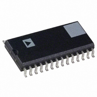
AD768ARZ Analog Devices Inc, AD768ARZ Datasheet - Page 4

AD768ARZ
Manufacturer Part Number
AD768ARZ
Description
IC DAC 16BIT 30MSPS 28-SOIC
Manufacturer
Analog Devices Inc
Datasheet
1.AD768ARZ.pdf
(20 pages)
Specifications of AD768ARZ
Data Interface
Parallel
Settling Time
25ns
Number Of Bits
16
Number Of Converters
1
Voltage Supply Source
Dual ±
Power Dissipation (max)
600mW
Operating Temperature
-40°C ~ 85°C
Mounting Type
Surface Mount
Package / Case
28-SOIC (7.5mm Width)
Resolution (bits)
16bit
Sampling Rate
30MSPS
Input Channel Type
Parallel
Supply Current
63mA
Digital Ic Case Style
SOIC
No. Of Pins
20
Supply Voltage Range - Analog
± 4.75V To ± 5.25V
Rohs Compliant
Yes
Number Of Channels
1
Resolution
16b
Interface Type
Parallel
Single Supply Voltage (typ)
Not RequiredV
Dual Supply Voltage (typ)
±5V
Architecture
R-2R/Current Steering
Power Supply Requirement
Dual
Output Type
Current
Integral Nonlinearity Error
±8LSB
Single Supply Voltage (min)
Not RequiredV
Single Supply Voltage (max)
Not RequiredV
Dual Supply Voltage (min)
±4.75V
Dual Supply Voltage (max)
±5.25V
Operating Temp Range
-40C to 85C
Operating Temperature Classification
Industrial
Mounting
Surface Mount
Pin Count
28
Package Type
SOIC W
Lead Free Status / RoHS Status
Lead free / RoHS Compliant
Lead Free Status / RoHS Status
Lead free / RoHS Compliant, Lead free / RoHS Compliant
Available stocks
Company
Part Number
Manufacturer
Quantity
Price
Part Number:
AD768ARZ
Manufacturer:
ADI/亚德诺
Quantity:
20 000
AD768
WAFER TEST LIMITS
Parameter
Integral Nonlinearity
Differential Nonlinearity
Offset Error
Gain Error
Reference Voltage
Positive Supply Current
Negative Supply Current
Power Dissipation
NOTES
1
2
3
4
Pin No.
1
2
3
4
5
6
7
8–14
15
16
17–23
24
25
26
27
28
Type: AI = Analog Input; DI = Digital Input; AO = Analog Output; P = Power.
Electrical test are performed at wafer probe to the limits shown. Due to variations in assembly methods and normal
yield loss, yield after packaging is not guaranteed for standard product dice.
Limits extrapolated from testing of individual bit errors.
Die offers latch control pad. Edge triggered latches become level triggered when latch control and clock pads are high.
Die substrate is connected to V
Symbol
IOUTA
NR
REFOUT
NC
REFCOM
IREFIN
DB0
DB1–DB7
DCOM
CLOCK
DB8–DB14
DB15
V
V
IOUTB
LADCOM
DD
EE
(LSB) DB0
REFCOM
REFOUT
PIN CONFIGURATION
IREFIN
IOUTA
2
DB1
DB2
DB3
DB4
DB5
DB6
DB7
NR
NC
2
EE.
10
11
12
13
14
1
2
3
4
5
6
7
8
9
NC = NO CONNECT
(Not to Scale)
TOP VIEW
1
AD768
Type
AO
AI
AO
NC
P
AI
DI
DI
P
DI
DI
DI
P
P
AO
P
(T
A
= +25 C, V
28
27
26
25
24
23
22
21
20
19
18
17
16
15
AD768ACHIPS Limit
40
73
600
LADCOM
IOUTB
V
V
DB15 (MSB)
DB14
DB13
DB12
DB11
DB10
DB9
DB8
CLOCK
DCOM
8
6
0.2
1.0
1.0
EE
DD
(–5V)
(+5V)
DAC Current Output. Full-scale current when all data bits are 1s.
Reference Output Voltage. Nominal value is 2.5 V.
Reference Input Current. Nominal is 5 mA. DAC full-scale is 4 this current.
Data Bits 1–7.
Clock Input. Data latched on positive edge of clock.
Data Bits 8–14.
Complementary DAC Current Output. Full-scale current when all data bits are 0s.
DAC Ladder Common.
Name and Function
Noise Reduction Node. Add capacitor for noise reduction.
No Connect. Reserved for internal use.
Reference Ground.
Data Bit 0 (LSB).
Digital Ground.
Data Bit 15 (MSB).
Positive Supply Voltage. Nominal is +5 V.
Negative Supply Voltage. Nominal is –5 V.
DD
= +5.0 V, V
PIN DESCRIPTIONS
EE
= –5.0 V, I
LADCOM
–4–
REFOUT
IOUTB
IOUTA
V
V
NR
NC
EE
EE
REFCOM IREFIN
REFIN
Units
LSB max
LSB max
% FSR max
% FSR max
% of nom. 2.5 V max
mA max
mA max
mW max
Die Size:
0.1106
(2.81
V
= 5 mA, unless otherwise noted)
DD
V
DD
3.60 mm, 10.116 sq. mm)
DICE CHARACTERISTICS
0.1417 inch, 15,672 sq. mils
DB15
DB0
DB14 DB13
DB1
DB2
DB12 DB11
DB3 DB4
3, 4
DB10
DB9
DB8
CLOCK
LATCH CONTROL
DCOM
DB7
DB6
DB5
REV. B


