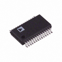
AD5544ARSZ Analog Devices Inc, AD5544ARSZ Datasheet - Page 4

AD5544ARSZ
Manufacturer Part Number
AD5544ARSZ
Description
IC DAC 16BIT QUAD SRL IN 28-SSOP
Manufacturer
Analog Devices Inc
Datasheet
1.AD5554BRSZ.pdf
(16 pages)
Specifications of AD5544ARSZ
Data Interface
Serial, SPI™
Settling Time
900ns
Number Of Bits
16
Number Of Converters
4
Voltage Supply Source
Dual ±
Power Dissipation (max)
1.25mW
Operating Temperature
-40°C ~ 125°C
Mounting Type
Surface Mount
Package / Case
28-SSOP
Resolution (bits)
16bit
Sampling Rate
500kSPS
Input Channel Type
Serial
Supply Voltage Range - Digital
2.7V To 5.5V
Supply Current
5µA
Digital Ic Case Style
SSOP
Lead Free Status / RoHS Status
Lead free / RoHS Compliant
Available stocks
Company
Part Number
Manufacturer
Quantity
Price
Part Number:
AD5544ARSZ
Manufacturer:
ADI/亚德诺
Quantity:
20 000
AD5544/AD5554
Parameter
AC CHARACTERISTICS
1
2
3
4
AD5554 ELECTRICAL CHARACTERISTICS
V
range of −40°C to +125°C, unless otherwise noted.
Table 2.
Parameter
STATIC PERFORMANCE
REFERENCE INPUT
ANALOG OUTPUT
LOGIC INPUT AND OUTPUT
INTERFACE TIMING
All static performance tests (except I
tied to the amplifier output. Typical values represent average readings measured at 25°C.
These parameters are guaranteed by design and not subject to production testing.
All input control signals are specified with t
All ac characteristic tests are performed in a closed-loop system using an
DD
Output Voltage Settling Time
Reference Multiplying BW
DAC Glitch Impulse
Feedthrough Error
Crosstalk Error
Digital Feedthrough
Total Harmonic Distortion
Output Spot Noise Voltage
Resolution
Relative Accuracy
Differential Nonlinearity
Output Leakage Current
Full-Scale Gain Error
Full-Scale Tempco
Feedback Resistor
V
Input Resistance
Input Resistance Match
Input Capacitance
Output Current
Output Capacitance
Logic Input Low Voltage
Logic Input High Voltage
Input Leakage Current
Input Capacitance
Logic Output Low Voltage
Logic Output High Voltage
Clock Width High
Clock Width Low
CS to Clock Setup
Clock to CS Hold
Clock to SDO Propagation
Load DAC Pulse Width
REF
= 2.7 V to 5.5 V, V
x Range
Delay
2, 3
2
2
2
4
2
1
SS
= 0 V, I
OUT
OUT
) are performed in a closed-loop system using an external precision
Symbol
t
BW − 3 dB
Q
V
V
Q
THD
e
x = virtual GND, A
Symbol
N
INL
DNL
I
I
G
TCV
R
V
R
R
C
I
C
V
V
I
C
V
V
t
t
t
t
t
t
OUT
OUT
OUT
IL
S
CH
CL
CSS
CSH
PD
LDAC
N
OUT
OUT
FB
REF
REF
REF
REF
OUT
IL
IH
IL
OL
OH
FSE
R
= t
x
x
x
x
x
x
x
x
x/V
A/V
FS
x
F
= 2.5 ns (10% to 90% of 3 V) and timed from a voltage level of 1.5 V.
REF
REF
x
B
Test Condition/Comments
V
To ±0.1% of full scale, data = 0x0000 to 0xFFFF to 0x0000
V
V
Data = 0x0000, V
Data = 0x0000, V
f = 100 kHz
CS = 1, f
f = 1 kHz, BW = 1 Hz
Test Condition/Comments
1 LSB = V
Data = 0x0000, T
Data = 0x0000, T
Data = 0x3FFF
V
Channel-to-channel
Data = 0x3FFF
Code dependent
I
I
OL
OH
REF
REF
REF
DD
= 1.6 mA
= 100 μA
x = 5 V p-p, data = 0xFFFF, C
x = 8 V, data = 0x0000 to 0x8000 to 0x0000
= 5 V
= 5 V p-p, data = 0xFFFF, f = 1 kHz
GND
CLK
x = 0 V, V
REF
= 1 MHz
/2
Rev. D | Page 4 of 16
AD8038
14
= 610 μV when V
A
A
REF
REF
= 25°C
= 85°C
REF
x = 100 mV rms, f = 100 kHz
B = 100 mV rms, adjacent channel,
I-to-V converter amplifier.
A = V
REF
B = V
FB
REF
= 2.0 pF,
= 10 V
REF
C = V
OP177
REF
I-to-V converter amplifier. The AD5544 R
D = 10 V, T
Min
25
0
25
Min
4
−15
4
1.25
2.4
4
25
2
25
A
= full operating temperature
Typ
0.9
12
−1
−65
−90
0.6
−98
7
Typ
±2
1
6
6
1
5
80
Max
Max
14
±0.5
±1
10
20
±10
8
+15
8
2.5
0.8
1
10
0.4
20
FB
terminal is
Unit
μs
MHz
nV-sec
dB
dB
nV-sec
dB
nV/√Hz
Unit
Bits
LSB
LSB
nA
nA
mV
ppm/°C
kΩ
V
kΩ
%
pF
mA
pF
V
V
μA
pF
V
V
ns
ns
ns
ns
ns
ns


