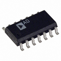
AD5542LRZ Analog Devices Inc, AD5542LRZ Datasheet - Page 4

AD5542LRZ
Manufacturer Part Number
AD5542LRZ
Description
IC DAC 16BIT SERIAL-IN 14-SOIC
Manufacturer
Analog Devices Inc
Specifications of AD5542LRZ
Data Interface
Serial
Design Resources
High Precision Digital-to-Analog Conversion Using the 16-Bit AD5542/1, ADR421, and AD8628 (CN0079) How to Achieve High Precision Voltage Level Setting Using AD5541A/42A (CN0169)
Settling Time
1µs
Number Of Bits
16
Number Of Converters
1
Voltage Supply Source
Single Supply
Power Dissipation (max)
6.05mW
Operating Temperature
-40°C ~ 85°C
Mounting Type
Surface Mount
Package / Case
14-SOIC (3.9mm Width), 14-SOL
Resolution (bits)
16bit
Sampling Rate
1.5MSPS
Input Channel Type
Serial
Supply Voltage Range - Analog
2.7V To 5.5V
Supply Current
300µA
Digital Ic Case Style
SOIC
Number Of Channels
1
Resolution
16b
Conversion Rate
1.5MSPS
Interface Type
SER 3W SPI QSPI UW
Single Supply Voltage (typ)
5V
Dual Supply Voltage (typ)
Not RequiredV
Architecture
R-2R
Power Supply Requirement
Single
Output Type
Voltage
Integral Nonlinearity Error
±1LSB
Single Supply Voltage (min)
4.5V
Single Supply Voltage (max)
5.5V
Dual Supply Voltage (min)
Not RequiredV
Dual Supply Voltage (max)
Not RequiredV
Operating Temp Range
0C to 70C
Operating Temperature Classification
Commercial
Mounting
Surface Mount
Pin Count
14
Package Type
SOIC N
Lead Free Status / RoHS Status
Lead free / RoHS Compliant
Lead Free Status / RoHS Status
Lead free / RoHS Compliant, Lead free / RoHS Compliant
Available stocks
Company
Part Number
Manufacturer
Quantity
Price
Company:
Part Number:
AD5542LRZ
Manufacturer:
Exar
Quantity:
46
Part Number:
AD5542LRZ
Manufacturer:
ADI/亚德诺
Quantity:
20 000
AD5541/AD5542
Parameter
POWER REQUIREMENTS
1
2
3
TIMING CHARACTERISTICS
V
+85°C, unless otherwise noted.
Table 3.
Parameter
f
t
t
t
t
t
t
t
t
t
t
t
t
t
1
2
SCLK
1
2
3
4
5
6
7
8
9
9
10
11
12
Temperature ranges are as follows: A, B, C versions: −40°C to +85°C; J, L versions: 0°C to 70°C.
Reference input resistance is code-dependent, minimum at 0x8555.
Guaranteed by design, not subject to production test.
Guaranteed by design and characterization. Not production tested
All input signals are specified with t
DD
V
I
Power Dissipation
DD
DD
= 2.7 V to 5.5 V ±10%, V
1
1, 2
LDAC*
*AD5542 ONLY. CAN BE TIED PERMANENTLY LOW IF REQUIRED.
SCLK
DIN
CS
Limit
25
40
20
20
10
15
30
20
15
4
7.5
30
30
30
t
12
REF
R
t
= t
6
= 2.5 V, V
F
= 1 ns/V and timed from a voltage level of (V
t
DB15
t
4
8
Unit
MHz max
ns min
ns min
ns min
ns min
ns min
ns min
ns min
ns min
ns min
ns min
ns min
ns min
ns min
t
5
INH
= 3 V and 90% of V
Min
2.7
Typ
125
0.625
t
2
Figure 3. Timing Diagram
Description
SCLK cycle frequency
SCLK cycle time
SCLK high time
SCLK low time
CS low to SCLK high setup
CS high to SCLK high setup
SCLK high to CS low hold time
SCLK high to CS high hold time
Data setup time
Data hold time (V
Data hold time (V
LDAC pulse width
CS high to LDAC low setup
CS high time between active periods
Rev. E | Page 4 of 20
t
1
DD
t
3
, V
INL
INL
+ V
= 0 V and 10% of V
Max
5.5
150
0.825
INH
)/2.
INH
INH
t
7
= 90% of V
= 3V, V
t
5
t
11
INL
t
10
Unit
V
μA
mW
= 0 V)
DD
DD
, V
, AGND = DGND = 0 V; −40°C < T
INL
= 10% of V
Test Conditions
Digital inputs at rails
DD
)
A
<


