AD420ANZ-32 Analog Devices Inc, AD420ANZ-32 Datasheet
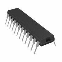
IC DAC SRL 16BIT 24-DIP

AD420ANZ-32

Manufacturer Part Number
AD420ANZ-32
Description
IC DAC SRL 16BIT 24-DIP
Manufacturer
Analog Devices Inc
Datasheets

Specifications of AD420ANZ-32

Data Interface
Serial
Settling Time
2.5µs
Number Of Bits
16
Number Of Converters
1
Voltage Supply Source
Single Supply
Power Dissipation (max)
176mW
Operating Temperature
-40°C ~ 85°C
Mounting Type
Through Hole
Package / Case
24-DIP (0.300", 7.62mm)
Resolution (bits)
16bit
Sampling Rate
400SPS
Input Channel Type
Serial
Supply Current
4.2mA
Digital Ic Case Style
DIP
No. Of Pins
24
Lead Free Status / RoHS Status
Lead free / RoHS Compliant
Lead Free Status / RoHS Status
Lead free / RoHS Compliant, Lead free / RoHS Compliant

Available stocks

Company
Part Number
Manufacturer
Quantity
Price
Part Number:
AD420ANZ-32
Manufacturer:
MICROCHIP
Quantity:
12
Part Number:
AD420ANZ-32
Manufacturer:
ADI
Quantity:
2 000
Part Number:
AD420ANZ-32
Manufacturer:
ADI
Quantity:
3 537
Part Number:
AD420ANZ-32
Manufacturer:
ADI/亚德诺
Quantity:
20 000
a
PRODUCT DESCRIPTION
The AD420 is a complete digital to current loop output con-
verter, designed to meet the needs of the industrial control
market. It provides a high precision, fully integrated, low cost
single-chip solution for generating current loop signals in a
compact 24-lead SOIC or PDIP package.
The output current range can be programmed to 4 mA–20 mA,
0 mA–20 mA or an overrange function of 0 mA–24 mA. The
AD420 can alternatively provide a voltage output from a sepa-
rate pin that can be configured to provide 0 V–5 V, 0 V–10 V,
amplifier.
The 3.3M Baud serial input logic design minimizes the cost of
galvanic isolation and allows for simple connection to com-
monly used microprocessors. It can be used in three-wire or
asynchronous mode and a serial-out pin is provided to allow
daisy chaining of multiple DACs on the current loop side of the
isolation barrier.
The AD420 uses sigma-delta (
16-bit monotonicity at very low cost. Full-scale settling to 0.1%
occurs within 3 ms. The only external components that are re-
quired (in addition to normal transient protection circuitry) are
two low cost capacitors which are used in the DAC output filter.
If the AD420 is going to be used at extreme temperatures and
supply voltages, an external output transistor can be used to
minimize power dissipation on the chip via the “BOOST” pin.
The FAULT DETECT pin signals when an open circuit occurs
in the loop. The on-chip voltage reference can be used to supply
a precision +5 V to external components in addition to the
AD420 or, if the user desires temperature stability exceeding
25 ppm/ C, an external precision reference such as the AD586
can be used as the reference.
SPI is a registered trademark of Motorola.
MICROWIRE is a registered trademark of National Semiconductor.
REV. F
Information furnished by Analog Devices is believed to be accurate and
reliable. However, no responsibility is assumed by Analog Devices for its
use, nor for any infringements of patents or other rights of third parties
which may result from its use. No license is granted by implication or
otherwise under any patent or patent rights of Analog Devices.
5 V or 10 V with the addition of a single external buffer
FEATURES
4 mA–20 mA, 0 mA–20 mA or 0 mA–24 mA Current Output
16-Bit Resolution and Monotonicity
Flexible Serial Digital Interface (3.3 MBPS)
On-Chip Loop Fault Detection
On-Chip 5 V Reference (25 ppm/ C Max)
Asynchronous CLEAR Function
Maximum Power Supply Range of 32 V
Output Loop Compliance of 0 V to V
24-Lead SOIC and PDIP Packages
0.012% Max Integral Nonlinearity
0.05% Max Offset (Trimmable)
0.15% Max Total Output Error (Trimmable)
) DAC technology to achieve
CC
– 2.5 V
One Technology Way, P.O. Box 9106, Norwood, MA 02062-9106, U.S.A.
Tel: 781/329-4700
Fax: 781/326-8703
The AD420 is available in a 24-lead SOIC and PDIP over the
industrial temperature range of –40 C to +85 C.
PRODUCT HIGHLIGHTS
1. The AD420 is a single chip solution for generating 4 mA–
2. The AD420 is specified with a power supply range
3. The flexible serial input can be used in three-wire mode
4. The serial data out pin can be used to daisy chain any num-
5. At power-up the AD420 initializes its output to the low end
6. The AD420 has an asynchronous CLEAR pin which sends
7. The AD420 BOOST pin accommodates an external transis-
8. The offset of 0.05% and total output error of 0.15% can
4 mA–20 mA, 0 mA–20 mA DAC
DATA OUT
SELECT 1
SELECT 2
REF OUT
DATA IN
20 mA or 0 mA–20 mA signals at the “controller end” of the
current loop.
from 12 V to 32 V. Output loop compliance is 0 V to
V
with SPI
chronous mode which minimizes the number of control
signals required.
ber of AD420s together in three-wire mode.
of the selected range.
the output to the low end of the selected range (0 mA,
4 mA, or 0 V).
tor to off-load power dissipation from the chip.
be trimmed if desired, using two external potentiometers.
CLEAR
CLOCK
RANGE
RANGE
LATCH
REF IN
CC
V
– 2.5 V.
LL
®
FUNCTIONAL BLOCK DIAGRAM
REGISTER
DATA I/P
or MICROWIRE
World Wide Web Site: http://www.analog.com
REFERENCE
OFFSET
CLOCK
16-BIT
TRIM
DAC
AD420
Serial Input 16-Bit
CAP 1
®
SWITCHED
FILTERING
CURRENT
SOURCES
microcontrollers, or in asyn-
4k
AND
V
CC
CAP 2
© Analog Devices, Inc., 1999
40
GND
1.25k
AD420
BOOST
I
V
FAULT
DETECT
OUT
OUT

Related parts for AD420ANZ-32

AD420ANZ-32 Summary of contents

Page 1

FEATURES 4 mA–20 mA, 0 mA– mA–24 mA Current Output 16-Bit Resolution and Monotonicity 0.012% Max Integral Nonlinearity 0.05% Max Offset (Trimmable) 0.15% Max Total Output Error (Trimmable) Flexible Serial Digital Interface (3.3 MBPS) On-Chip Loop ...

Page 2

AD420–SPECIFICATIONS Parameter RESOLUTION I CHARACTERISTICS OUT Operating Current Ranges Current Loop Voltage Compliance 2 Settling Time (to 0.1% of FS) Output Impedance (Current Mode) 3 Accuracy Monotonicity Integral Nonlinearity Offset ( mA + ...

Page 3

ABSOLUTE MAXIMUM RATINGS GND CC AD420AR/AN- ...

Page 4

AD420 Timing Requirements (T = – + THREE-WIRE INTERFACE CLOCK WORD "N" DATA LATCH WORD "N – 1" DATA OUT t CK ...

Page 5

Pin # Symbol 1, 12, 13 FAULT DETECT 4 RANGE SELECT 2 5 RANGE SELECT 1 6 CLEAR 7 LATCH 8 CLOCK 9 DATA IN 10 DATA OUT 11 GND 14 REF OUT 15 ...

Page 6

AD420 THEORY OF OPERATION The AD420 uses a sigma-delta ( ) architecture to carry out the digital-to-analog conversion. This architecture is particularly well suited for the relatively low bandwidth requirements of the industrial control environment because of its inherent monoto- ...

Page 7

APPLICATIONS CURRENT OUTPUT The AD420 can provide 4 mA–20 mA, 0 mA–20 mA mA– output without any active external components. Filter capacitors C1 and C2 can be any type of low cost ceramic ca- pacitors. To ...

Page 8

AD420 THREE-WIRE INTERFACE Figure 8 shows the AD420 connected in the three-wire interface mode. The AD420 data input block contains a serial input shift register and a parallel latch. The contents of the shift register are controlled by the DATA ...

Page 9

MICROPROCESSOR INTERFACE SECTION AD420-TO-MC68HC11 (SPI BUS) INTERFACE The AD420 interface to the Motorola SPI (Serial Peripheral Interface) is shown in Figure 10. The MOSI, SCK, and SS pins of the HC11 are respectively connected to the DATA IN, CLOCK, and ...

Page 10

AD420 AD420 PROTECTION TRANSIENT VOLTAGE PROTECTION The AD420 contains ESD protection diodes which prevent damage from normal handling. The industrial control environ- ment can, however, subject I/O circuits to much higher tran- sients. In order to protect the AD420 from ...

Page 11

MAX 0.200 (5.05) 0.125 (3.18) 0.0118 (0.30) 0.0040 (0.10) REV. F OUTLINE DIMENSIONS Dimensions shown in inches and (mm). 24-Lead Plastic DIP (N-24) 1.275 (32.30) 1.125 (28.60 0.280 (7.11) 0.240 (6.10 0.060 (1.52) PIN ...

Related keywords