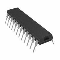
AD7537JNZ Analog Devices Inc, AD7537JNZ Datasheet - Page 2

AD7537JNZ
Manufacturer Part Number
AD7537JNZ
Description
IC DAC 12BIT LC2MOS DUAL 24-DIP
Manufacturer
Analog Devices Inc
Datasheet
1.AD7537JNZ.pdf
(8 pages)
Specifications of AD7537JNZ
Data Interface
Parallel
Settling Time
250µs
Number Of Bits
12
Number Of Converters
2
Voltage Supply Source
Single Supply
Power Dissipation (max)
24mW
Operating Temperature
-40°C ~ 85°C
Mounting Type
Through Hole
Package / Case
24-DIP (0.300", 7.62mm)
Resolution (bits)
12bit
Sampling Rate
667kSPS
Input Channel Type
Parallel
Supply Current
2mA
Digital Ic Case Style
DIP
No. Of Pins
24
Lead Free Status / RoHS Status
Lead free / RoHS Compliant
Available stocks
Company
Part Number
Manufacturer
Quantity
Price
Part Number:
AD7537JNZ
Manufacturer:
ADI/亚德诺
Quantity:
20 000
Parameter
ACCURACY
REFERENCE INPUT
DIGITAL INPUTS
POWER SUPPLY
AC PERFORMANCE CHARACTERISTICS
These characteristics are included for Design Guidance only and are not subject to test.
(V
Parameter
Output Current Settling Time
Digital-to-Analog Glitch lmpulse
AC Feedthrough
Power Supply Rejection
Output Capacitance
Channel-to-Channel Isolation
Digital Crosstalk
Output Noise Voltage Density
Total Harmonic Distortion
NOTES
1
Specifications subject to change without notice.
AD7537–SPECIFICATIONS
Temperature range as follows:
DD
Resolution
Relative Accuracy
Differential Nonlinearity
Gain Error
Gain Temperature Coefficient
Output Leakage Current
Input Resistance
V
V
V
I
C
V
I
V
V
C
C
C
C
V
V
(10 Hz–100 kHz)
IN
DD
REFA
IH
IIL
DD
IN
Gain/ V
REFA
REFB
REFA
REFB
OUTA
OUTB
OUTA
OUTB
= +12 V to +15 V; V
I
I
Input Resistance Match
+25 C
T
(Input Current)
OUTA
OUTB
(lnput High Voltage)
Gain/ Temperature
(lnput Capacitance)
(Input Low Voltage)
MIN
+25 C
T
+25 C
T
, V
MIN
MIN
to I
to I
to I
to I
to T
REFB
OUTB
OUTA
OUTA
DD
OUTB
to T
to T
MAX
4
MAX
MAX
3
2
REFA
J, K, L Versions: –40 C to +85 C;
A, B, C Versions: –40 C to +85 C;
S, T, U Versions: –55 C to +125 C
= V
2
;
REFB
T
1.5
7
–70
–70
70
70
140
140
–84
–84
7
25
–82
A
0.01
J, A
Versions
12
10
150
10
150
9
20
2.4
0.8
10
10.8/16.5 10.8/16.5 10.8/16.5 10.8/16.5 10.8/16.5 10.8/16.5 V min/V max
2
= +25 C
= +10 V; I
1
1
6
5
3
1
10
K, B
Versions
12
10
150
10
150
9
20
2.4
0.8
10
2
OUTA
T
–65
–65
70
70
140
140
1/2
1
3
5
3
1
10
0.02
A
= T
= AGNDA = 0 V, I
MIN
, T
L, C
Versions
12
10
150
10
150
9
20
2.4
0.8
10
2
1/2
1
1
5
1
1
10
(V
MAX
I
OUTB
DD
= +12 V to +15 V,
= AGNDB = 0 V. All specifications T
2
3
4
Units
nV-s typ
dB max
dB max
% per % max
pF max
pF max
pF max
pF max
dB typ
dB typ
nV-s typ
nV/ Hz typ
dB typ
Sample tested at +25 C to ensure compliance.
Functional at V
Pin 12 (DGND) on ceramic DIPs is connected to lid.
s max
S
Version
12
10
250
10
250
9
20
2.4
0.8
10
2
OUTB
1
1
6
5
3
1
10
–2–
= AGNDB = 0 V. Output Amplifiers are AD644 except where noted.)
DD
T
Version
12
10
250
10
250
9
20
2.4
0.8
10
2
Test Conditions/Comments
To 0.01% of full-scale range. I
DAC output measured from falling edge of WR.
Typical Value of Settling Time is 0.8 s.
Measured with V
C
V
DAC registers loaded with all 0s.
DAC A, DAC B loaded with all 0s
DAC A, DAC B loaded with all 1s
V
Both DACs loaded with all 1s.
V
Both DACs loaded with all 1s.
Measured for a Code Transition of all 0s to all 1s.
I
Measured between R
Frequency of measurement is 10 Hz–100 kHz.
V
1/2
1
3
5
3
1
10
OUTA
V
REFA
REFA
REFB
IN
EXT
= 5 V, with degraded specifications.
DD
= 6 V rms, 1 kHz. Both DACs loaded with all 1s.
, I
10%, V
= 13 pF. DAC registers alternately loaded with all 0s and all 1s.
, V
= V
= 20 V p-p 10 kHz sine wave, V
= 20 V p-p 10 kHz sine wave, V
OUTB
REFB
DD
U
Version
12
10
250
10
250
9
20
2.4
0.8
10
2
1/2
1
2
5
1
1
10
load = 100 , C
max – V
= 20 V p-p 10 kHz sine wave.
REFA
REFA
= V
FBA
DD
= V
REFB
Units
Bits
LSB max
LSB max
LSB max
ppm/ C max Typical value is 1 ppm/ C
nA max
nA max
nA max
nA max
k min
k max
% max
V min
V max
pF max
mA max
MIN
A max
A max
min
and I
REFB
to T
= 10 V; I
EXT
OUTA
OUT
= 0 V. I
MAX
= 13 pF.
unless otherwise noted.)
load = 100 , C
or R
OUTA
Test Conditions/Comments
All grades guaranteed mono-
tonic over temperature.
Measured using R
Both DAC registers loaded
with all 1s.
DAC A Register loaded
with all 0s
DAC B Register loaded
with all 0s
Typical Input Resistance = 14 k
Typically 0.5%
V
OUTA
REFB
REFA
IN
FBB
= AGND = 0 V,
= V
= 0 V.
, I
= 0 V.
and I
OUTB
DD
OUTB.
load = 100 ,
EXT
= 13 pF.
FBA
, R
FBB
REV. 0
.


