AD9761ARSZ Analog Devices Inc, AD9761ARSZ Datasheet
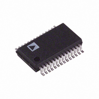
IC DAC 10BIT DUAL 40MSPS 28-SSOP

AD9761ARSZ

Manufacturer Part Number
AD9761ARSZ
Description
IC DAC 10BIT DUAL 40MSPS 28-SSOP
Manufacturer
Analog Devices Inc
Datasheet

Specifications of AD9761ARSZ

Data Interface
Parallel
Settling Time
35ns
Number Of Bits
10
Number Of Converters
2
Voltage Supply Source
Analog and Digital
Power Dissipation (max)
250mW
Operating Temperature
-40°C ~ 85°C
Mounting Type
Surface Mount
Package / Case
28-SSOP
Resolution (bits)
10bit
Sampling Rate
40MSPS
Input Channel Type
Parallel
Supply Voltage Range - Analogue
3V To 5.5V
Supply Voltage Range - Digital
2.7V To 5.5V
Supply
RoHS Compliant
Lead Free Status / RoHS Status
Lead free / RoHS Compliant
For Use With
AD9761-EBZ - BOARD EVAL FOR AD9761
Lead Free Status / RoHS Status
Lead free / RoHS Compliant

Available stocks

Company
Part Number
Manufacturer
Quantity
Price
Part Number:
AD9761ARSZ
Manufacturer:
ADI/亚德诺
Quantity:
20 000
PRODUCT DESCRIPTION
The AD9761 is a complete dual-channel, high speed, 10-bit
CMOS DAC. The AD9761 has been developed specifically for
use in wide bandwidth communication applications (e.g., spread
spectrum) where digital I and Q information is being processed
during transmit operations. It integrates two 10-bit, 40 MSPS
DACs, dual 2 interpolation filters, a voltage reference, and digi-
tal input interface circuitry. The AD9761 supports a 20 MSPS
per channel input data rate that is then interpolated by 2 up to
40 MSPS before simultaneously updating each DAC.
The interleaved I and Q input data stream is presented to the
digital interface circuitry, which consists of I and Q latches as
well as some additional control logic. The data is de-interleaved
back into its original I and Q data. An on-chip state machine
ensures the proper pairing of I and Q data. The data output from
each latch is then processed by a 2 digital interpolation filter
that eases the reconstruction filter requirements. The interpo-
lated output of each filter serves as the input of their respective
10-bit DAC.
The DACs utilize a segmented current source architecture com-
bined with a proprietary switching technique to reduce glitch
energy and to maximize dynamic accuracy. Each DAC provides
differential current output, thus supporting single-ended or dif-
ferential applications. Both DACs are simultaneously updated
and provide a nominal full-scale current of 10 mA. Also, the
full-scale currents between each DAC are matched to within
0.07 dB (i.e., 0.75%), thus eliminating the need for additional
gain calibration circuitry.
The AD9761 is manufactured on an advanced low cost CMOS
process. It operates from a single supply of 3 V to 5.5 V and
consumes 200 mW of power. To make the AD9761 complete, it
also offers an internal 1.20 V temperature-compensated band gap
reference.
REV. C
Information furnished by Analog Devices is believed to be accurate and
reliable. However, no responsibility is assumed by Analog Devices for its
use, nor for any infringements of patents or other rights of third parties
that may result from its use. No license is granted by implication or oth-
erwise under any patent or patent rights of Analog Devices.Trademarks
and registered trademarks are the property of their respective companies.
FEATURES
Complete 10-Bit, 40 MSPS Dual Transmit DAC
Excellent Gain and Offset Matching
Differential Nonlinearity Error: 0.5 LSB
Effective Number of Bits: 9.5
Signal-to-Noise and Distortion Ratio: 59 dB
Spurious-Free Dynamic Range: 71 dB
2 Interpolation Filters
20 MSPS/Channel Data Rate
Single Supply: 3 V to 5.5 V
Low Power Dissipation: 93 mW (3 V Supply @
On-Chip Reference
28-Lead SSOP
40 MSPS)
PRODUCT HIGHLIGHTS
1. Dual 10-Bit, 40 MSPS DACs
2. 2 Digital Interpolation Filters
3. Low Power
4. On-Chip Voltage Reference
5. Single 10-Bit Digital Input Bus
6. Small Package
7. Product Family
One Technology Way, P .O. Box 9106, Norwood, MA 02062-9106, U.S.A.
Tel: 781/329-4700
Fax: 781/326-8703
with 2 Interpolation Filters
The AD9761 includes a 1.20 V temperature-compensated
The AD9761 features a flexible digital interface that allows
The AD9761 offers the complete integrated function in a
The AD9761 Dual Transmit DAC has a pair of Dual Receive
A pair of high performance 40 MSPS DACs optimized for low
distortion performance provide for flexible transmission of I
and Q information.
Dual matching FIR interpolation filters with 62.5 dB stop-
band rejection precede each DAC input, thus reducing the
DACs’ reconstruction filter requirements.
Complete CMOS dual DAC function operates on a low
200 mW on a single supply from 3 V to 5.5 V. The DAC
full-scale current can be reduced for lower power opera-
tion, and a sleep mode is provided for power reduction
during idle periods.
band gap voltage reference.
each DAC to be addressed in a variety of ways including dif-
ferent update rates.
compact 28-lead SSOP package.
ADC companion products, the AD9281 (8 bits) and AD9201
(10 bits).
SELECT INPUT
WRITE INPUT
DAC DATA
(10 BITS)
INPUTS
SLEEP
FUNCTIONAL BLOCK DIAGRAM
DCOM
Dual 10-Bit TxDAC+
CONTROL
© 2003 Analog Devices, Inc. All rights reserved.
MUX
LATCH
LATCH
DVDD
Q
I
CLOCK
2
2
GENERATOR
REFERENCE
AD9761
ACOM
BIAS
AD9761
DAC
DAC
Q
I
AVDD
www.analog.com
REFLO
FSADJ
REFIO
COMP1
COMP2
COMP3
QOUTA
QOUTB
IOUTA
IOUTB
®

Related parts for AD9761ARSZ

AD9761ARSZ Summary of contents

Page 1

FEATURES Complete 10-Bit, 40 MSPS Dual Transmit DAC Excellent Gain and Offset Matching Differential Nonlinearity Error: 0.5 LSB Effective Number of Bits: 9.5 Signal-to-Noise and Distortion Ratio Spurious-Free Dynamic Range 2 Interpolation Filters 20 MSPS/Channel Data ...

Page 2

AD9761–SPECIFICATIONS DC SPECIFICATIONS ( MIN Parameter RESOLUTION DC ACCURACY 1 Integral Nonlinearity Error (INL 25° MIN MAX Differential Nonlinearity (DNL 25° MIN MAX Monotonicity (10-Bit) ANALOG ...

Page 3

DYNAMIC SPECIFICATIONS Parameter DYNAMIC PERFORMANCE Maximum Output Update Rate Output Settling Time (t to 0.025%) ST Output Propagation Delay ( Glitch Impulse Output Rise Time (10% to 90%) Output Fall Time (10% to 90%) AC LINEARITY TO NYQUIST ...

Page 4

AD9761 DIGITAL FILTER SPECIFICATIONS Parameter MAXIMUM INPUT CLOCK RATE (f DIGITAL FILTER CHARACTERISTICS 1 Pass Bandwidth : 0.005 dB Pass Bandwidth: 0.01 dB Pass Bandwidth: 0.1 dB Pass Bandwidth: –3 dB Linear Phase (FIR Implementation) Stop-Band Rejection: 0 ...

Page 5

ORDERING GUIDE Package Model Description AD9761ARS 28-Lead Shrink Small Outline (SSOP) RS-28 AD9761ARSRL 28-Lead Shrink Small Outline (SSOP) RS-28 AD9761-EB Evaluation Board ABSOLUTE MAXIMUM RATINGS* Parameter AVDD DVDD ACOM AVDD CLOCK, WRITE SELECT, SLEEP Digital Inputs IOUTA, IOUTB QOUTA, QOUTB ...

Page 6

AD9761 Pin No. Mnemonic Description 1 DB9 Most Significant Data Bit (MSB). 2–9 DB8–DB1 Data Bits 1–8. 10 DB0 Least Significant Data Bit (LSB). 11 CLOCK Clock Input. Both DACs’ outputs updated on positive edge of clock and digital filters ...

Page 7

DEFINITIONS OF SPECIFICATIONS Linearity Error (Also Called Integral Nonlinearity or INL) Linearity error is defined as the maximum deviation of the actual analog output from the ideal output, determined by a straight line drawn from zero to full scale. Differential ...

Page 8

AD9761—Typical Performance Characteristics Typical AC Characterization Curves @ 5 V Supplies (AVDD = 5 V, DVDD =  Doubly Terminated Load, T performance shown.) 0 –10 –20 –30 –40 –50 –60 –70 –80 –90 –100 START: 0Hz ...

Page 9

Typical AC Characterization Curves @ 3 V Supplies (AVDD = 3 V, DVDD =  Doubly Terminated Load, T performance shown.) 0 –10 –20 –30 –40 –50 –60 –70 –80 –90 START: 0Hz STOP: 10MHz TPC 10. ...

Page 10

AD9761 FUNCTIONAL DESCRIPTION Figure 4 shows a simplified block diagram of the AD9761. The AD9761 is a complete dual-channel, high speed, 10-bit CMOS DAC capable of operating MHz clock rate. It has been optimized for the ...

Page 11

Referring to Figure 5, the “new” first image associated with the DAC’s higher data rate after interpolation ...

Page 12

AD9761 REFLO AVDD +1.2V REF EXT. REFIO V REF FSADJ R SET I = REF V /R REF SET AD9761 Figure 7. External Reference Configuration REFERENCE CONTROL AMPLIFIER The AD9761 also contains an internal control amplifier that is used to ...

Page 13

The positive output compliance range is slightly dependent on the full-scale output current degrades slightly from OUTFS its nominal 1.25 V for 1.00 V for an OUTFS mA. ...

Page 14

AD9761 result, the digital inputs can also accommodate TTL levels when DVDD is set to accommodate the maximum high level voltage the TTL drivers. A DVDD OH(MAX) to 3.3 V will typically ensure proper ...

Page 15

RATIO (f /f OUT CLK Figure 16. I vs. Ratio @ DVDD = 3 V DVDD APPLYING THE AD9761 Output Configurations The following sections ...

Page 16

AD9761 The differential circuit shown in Figure 19 provides the neces- sary level-shifting required in a single-supply system. In this case, AVDD, which is the positive analog supply for both the AD9761 and the op amp, is also used to ...

Page 17

Maintaining low noise on power supplies and ground is critical to obtaining optimum results from the AD9761. If properly implemented, ground planes can perform a host of functions on high speed circuit boards such as bypassing, shielding, current transport. In ...

Page 18

AD9761 Figure 24a. Evaluation Board Schematic –18– REV. C ...

Page 19

REV. C Figure 24b. Evaluation Board Schematic –19– AD9761 ...

Page 20

AD9761 Figure 25. Silkscreen Layer—Top Figure 26. Component Side PCB Layout (Layer 1) –20– REV. C ...

Page 21

REV. C Figure 27. Ground Plane PCB Layout (Layer 2) Figure 28. Power Plane PCB Layout (Layer 3) –21– AD9761 ...

Page 22

AD9761 Figure 29. Solder Side PCB Layout (Layer 4) Figure 30. Silkscreen Layer—Bottom –22– REV. C ...

Page 23

MAX 0.05 MIN REV. C OUTLINE DIMENSIONS 28-Lead Shrink Small Outline Package [SSOP] (RS-28) Dimensions shown in millimeters 10.50 10.20 9. 5.60 8.20 5.30 7.80 5.00 7. 1.85 1.75 0.10 1.65 COPLANARITY 0.25 0.09 0.65 ...

Page 24

AD9761 Revision History Location 6/03—Data Sheet changed from REV REV. C. Renumbered TPCs and subsequent figures . . . . . . . . . . . . . . . . . . . . . . ...

Related keywords