AD7545AKNZ Analog Devices Inc, AD7545AKNZ Datasheet - Page 2
AD7545AKNZ
Manufacturer Part Number
AD7545AKNZ
Description
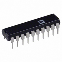
IC DAC 12BIT MULTIPLYING 20-DIP
Manufacturer
Analog Devices Inc
Specifications of AD7545AKNZ
Data Interface
Parallel
Settling Time
2µs
Number Of Bits
12
Number Of Converters
1
Voltage Supply Source
Single Supply
Operating Temperature
0°C ~ 70°C
Mounting Type
Through Hole
Package / Case
20-DIP (0.300", 7.62mm)
Resolution (bits)
12bit
Input Channel Type
Parallel
Supply Current
2mA
Digital Ic Case Style
DIP
No. Of Pins
20
Operating Temperature Range
0°C To +70°C
Lead Free Status / RoHS Status
Lead free / RoHS Compliant
Power Dissipation (max)
-
Lead Free Status / Rohs Status
RoHS Compliant part
Electrostatic Device
Available stocks
Company
Part Number
Manufacturer
Quantity
Price
Company:

Part Number:
AD7545AKNZ
Manufacturer:
2002+
Quantity:
6 219


AD7545–SPECIFICATIONS
Parameter
STATIC PERFORMANCE
DYNAMIC PERFORMANCE
REFERENCE INPUT
ANALOG OUTPUT
DIGITAL INPUTS
SWITCHING CHARACTERISTICS
POWER SUPPLY
NOTES
1
2
3
4
5
6
7
Specifications subject to change without notice.
Temperature range as follows: J, K, L, GL versions, 0°C to +70°C; A, B, C, GC versions, –25°C to +85°C; S, T, U GU versions, –55°C to +125°C.
This includes the effect of 5 ppm max gain TC.
Guaranteed but not tested.
DB0–DB11 = 0 V to V
Feedthrough can be further reduced by connecting the metal lid on the ceramic package (Suffix D) to DGND.
Logic inputs are MOS gates. Typical input current (+25°C) is less than 1 nA.
Sample tested at +25°C to ensure compliance.
Resolution
Differential Nonlinearity
Gain Error (Using Internal RFB)
Gain Temperature Coefficient
DC Supply Rejection
Output Leakage Current at OUT1
Current Settling Time
Propagation Delay
Digital-to-Analog Glitch Inpulse
AC Feedthrough
Input Resistance
Output Capacitance
Input High Voltage
Input Low Voltage
Input Current
Input Capacitance
Chip Select to Write Setup Time
Chip Select to Write Hold Time
Write Pulse Width
Data Setup Time
Data Hold Time
I
DD
∆Gain/∆Temperature
∆Gain/∆V
Input Change to 90%
of Final Analog Output)
At OUT1
(Pin 19 to GND)
C
C
V
V
I
DB0–DB11
WR, CS
t
t
t
t
t
IN
CS
CH
WR
DS
DH
IH
IL
OUT1
OUT1
DD
6
5
3
3
DD
(from Digital
3
3
3
or V
DD
to 0 V.
3
2
7
Version
All
J, A, S
K, B, T
L, C, U
GL, GC, GU
J, A, S
K, B, T
L, C, U
GL, GC, GU
J, A, S
K, B, T
L, C, U
GL, GC, GU
All
All
J, K, L, GL
A, B, C, GC
S, T, U, GU
All
All
All
All
All
All
All
All
All
All
All
All
All
All
All
All
All
T
12
± 2
± 1
± 1/2
± 1/2
± 4
± 1
± 1
± 1
± 20
± 10
± 5
± 1
± 5
0.015
10
10
10
2
300
400
5
7
25
70
200
2.4
0.8
± 1
5
20
280
200
0
250
175
140
100
10
2
100
10
A
= + 25 C T
V
DD
Limits
(V
= +5 V
REF
12
± 2
± 1
± 1/2
± 1/2
± 4
± 1
± 1
± 1
± 20
± 10
± 6
± 2
± 5
0.03
50
50
200
2
–
–
5
7
25
70
200
2.4
0.8
± 10
5
20
380
270
0
400
280
210
150
10
2
500
10
MIN,
= +10 V, V
T
MAX
1
–2–
T
12
± 2
± 1
± 1/2
± 1/2
± 4
± 1
± 1
± 1
± 25
± 15
± 10
± 6
± 10
0.01
10
10
10
2
250
250
5
7
25
70
200
13.5
1.5
± 1
5
20
180
120
0
160
100
90
60
10
2
100
10
OUT1
A
= + 25 C T
V
= O V, AGND = DGND unless otherwise noted)
DD
Limits
= +15 V
12
± 2
± 1
± 1/2
± 1/2
± 4
± 1
± 1
± 1
± 25
± 15
± 10
± 7
± 10
0.02
50
50
200
2
–
–
5
7
25
70
200
13.5
1.5
± 10
5
20
200
150
0
240
170
120
80
10
2
500
10
MIN,
T
MAX
1
Units
Bits
LSB max
LSB max
LSB max
LSB max
LSB max
LSB max
LSB max
LSB max
LSB max
LSB max
LSB max
LSB max
ppm/°C max
% per % max
nA max
nA max
nA max
µs max
ns max
nV sec typ
mV p-p typ
kΩ min
pF max
pF max
V min
V max
µA max
pF max
pF max
ns typ
ns min
ns min
ns typ
ns min
ns typ
ns min
mA max
µA max
µA typ
kΩ max
ns min
Test Conditions/Comments
10-Bit Monotonic T
12-Bit Monotonic T
12-Bit Monotonic T
12-Bit Monotonic T
DAC Register Loaded with
Gain Error Is Adjustable Using
the Circuits of Figures 4, 5, and 6
Typical Value is 2 ppm/°C for V
∆V
DB0–DB11 = 0 V; WR, CS = 0 V
To 1/2 LSB. OUT1 Load = 100 Ω. DAC
Output Measured from Falling Edge of
WR, CS = 0.
OUT1 Load = 100 Ω, C
V
V
Input Resistance TC = –300 ppm/°C typ
Typical Input Resistance = 11 kΩ
DB0–DB11 = 0 V, WR, CS = 0 V
DB0–DB11 = V
V
V
t
All Digital Inputs V
All Digital Inputs 0 V to V
All Digital Inputs 0 V to V
1111 1111 1111
V
See Timing Diagram
CS
REF
REF
IN
IN
IN
DD
≥ t
= 0 or V
= 0
= 0
= AGND
= ± 10 V, 10 kHz Sinewave
= ± 5%
WR
, t
CH
DD
≥ 0
DD
, WR, CS = 0 V
IL
MIN
MIN
MIN
MIN
or V
to T
to T
to T
to T
EXT
IH
DD
DD
= 13 pF
MAX
MAX
MAX
MAX
DD
REV. A
= +5 V
4
Related parts for AD7545AKNZ
Image
Part Number
Description
Manufacturer
Datasheet
Request
R

Part Number:
Description:
±1.7g Dual-Axis IMEMS Accelerometer Evaluation Board
Manufacturer:
Analog Devices Inc
Datasheet:

Part Number:
Description:
Inertial Sensor Evaluation System
Manufacturer:
Analog Devices Inc
Datasheet:
Part Number:
Description:
Manufacturer:
Analog Devices Inc
Datasheet:
Part Number:
Description:
Manufacturer:
Analog Devices Inc
Datasheet:
Part Number:
Description:
Manufacturer:
Analog Devices Inc
Datasheet:
Part Number:
Description:
Manufacturer:
Analog Devices Inc
Datasheet:
Part Number:
Description:
Manufacturer:
Analog Devices Inc
Datasheet:
Part Number:
Description:
Manufacturer:
Analog Devices Inc
Datasheet:
Part Number:
Description:
Manufacturer:
Analog Devices Inc
Datasheet:
Part Number:
Description:
Manufacturer:
Analog Devices Inc
Datasheet:
Part Number:
Description:
Manufacturer:
Analog Devices Inc
Datasheet:
Part Number:
Description:
Manufacturer:
Analog Devices Inc
Datasheet:
Part Number:
Description:
Manufacturer:
Analog Devices Inc
Datasheet: