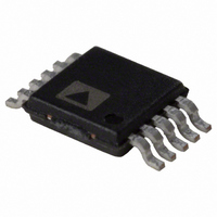
AD5624RBRMZ-3 Analog Devices Inc, AD5624RBRMZ-3 Datasheet - Page 20

AD5624RBRMZ-3
Manufacturer Part Number
AD5624RBRMZ-3
Description
IC DAC NANO 12BIT 1.25V 10-MSOP
Manufacturer
Analog Devices Inc
Series
nanoDAC™r
Specifications of AD5624RBRMZ-3
Data Interface
DSP, MICROWIRE™, QSPI™, Serial, SPI™
Settling Time
3µs
Number Of Bits
12
Number Of Converters
4
Voltage Supply Source
Single Supply
Operating Temperature
-40°C ~ 105°C
Mounting Type
Surface Mount
Package / Case
10-MSOP, Micro10™, 10-uMAX, 10-uSOP
Resolution (bits)
12bit
Sampling Rate
287kSPS
Input Channel Type
Serial
Supply Voltage Range - Analog
2.7V To 3.6V, 4.5V To 5.5V
Supply Current
950µA
Lead Free Status / RoHS Status
Lead free / RoHS Compliant
Power Dissipation (max)
-
Lead Free Status / RoHS Status
Lead free / RoHS Compliant, Lead free / RoHS Compliant
Available stocks
Company
Part Number
Manufacturer
Quantity
Price
Part Number:
AD5624RBRMZ-3
Manufacturer:
ADI/亚德诺
Quantity:
20 000
AD5624R/AD5644R/AD5664R
THEORY OF OPERATION
DIGITAL-TO-ANALOG SECTION
The AD5624R/AD5644R/AD5664R DACs are fabricated on a
CMOS process. The architecture consists of a string DAC
followed by an output buffer amplifier. Figure 50 shows a block
diagram of the DAC architecture.
Because the input coding to the DAC is straight binary, the ideal
output voltage when using an external reference is given by
The ideal output voltage when using the internal reference is
given by
where:
D is the decimal equivalent of the binary code that is loaded to
the DAC register:
N is the DAC resolution.
RESISTOR STRING
The resistor string is shown in Figure 51. It is simply a string of
resistors, each of value R. The code loaded to the DAC register
determines at which node on the string the voltage is tapped off
to be fed into the output amplifier. The voltage is tapped off by
closing one of the switches connecting the string to the
amplifier. Because it is a string of resistors, it is guaranteed
monotonic.
OUTPUT AMPLIFIER
The output buffer amplifier can generate rail-to-rail voltages on
its output, which gives an output range of 0 V to V
a load of 2 kΩ in parallel with 1000 pF to GND. The source and
sink capabilities of the output amplifier can be seen in Figure 33
and Figure 34. The slew rate is 1.8 V/μs with a ¼ to ¾ full-scale
settling time of 7 μs.
0 to 4095 for AD5624R (12 bit).
0 to 16,383 for AD5644R (14 bit).
0 to 65,535 for AD5664R (16 bit).
V
V
OUT
OUT
REGISTER
=
=
DAC
V
2
×
REFIN
V
REFOUT
⎛ ×
Figure 50. DAC Architecture
⎜
⎝
2
V
D
REFIN
N
⎛ ×
⎜
⎝
⎞
⎟
⎠
RESISTOR
2
STRING
D
N
GND
V
DD
⎞
⎟
⎠
REF
OUTPUT
AMPLIFIER
(GAIN = +2)
DD
V
. It can drive
OUT
Rev. B | Page 20 of 28
INTERNAL REFERENCE
The AD5624R/AD5644R/AD5664R on-chip reference is off at
power-up and is enabled via a write to a control register. See the
Internal Reference Setup section for details.
The AD56x4R-3 has a 1.25 V, 5 ppm/°C reference giving a full-
scale output of 2.5 V. The AD56x4R-5 has a 2.5 V, 5 ppm/°C
reference giving a full-scale output of 5 V. The internal reference
associated with each part is available at the V
is required if the reference output is used to drive external loads.
When using the internal reference, it is recommended that a
100 nF capacitor is placed between reference output and GND
for reference stability.
EXTERNAL REFERENCE
The V
use of an external reference if the application requires it. The
default condition of the on-chip reference is off at power-up. All
devices (AD56x4R-3 and the AD56x4R-5) can be operated from
a single 2.7 V to 5.5 V supply.
SERIAL INTERFACE
The AD5624R/AD5644R/AD5664R have a 3-wire serial interface
( SYNC , SCLK, and DIN) that is compatible with SPI, QSPI, and
MICROWIRE interface standards as well as with most DSPs. See
Figure 2
The write sequence begins by bringing the SYNC line low. Data
from the DIN line is clocked into the 24-bit shift register on the
falling edge of SCLK. The serial clock frequency can be as high
as 50 MHz, making the AD5624R/AD5644R/AD5664R compat-
ible with high speed DSPs. On the 24
last data bit is clocked in and the programmed function is
executed, that is, a change in DAC register contents and/or a
change in the mode of operation.
REFIN
for a timing diagram of a typical write sequence.
pin on the AD56x4R-3 and AD56x4R-5 allows the
R
R
R
R
R
Figure 51. Resistor String
th
TO OUTPUT
AMPLIFIER
falling clock edge, the
REFOUT
pin. A buffer


