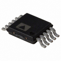
AD5624RBRMZ-5 Analog Devices Inc, AD5624RBRMZ-5 Datasheet - Page 7

AD5624RBRMZ-5
Manufacturer Part Number
AD5624RBRMZ-5
Description
IC DAC NANO 12BIT 2.5V 10-MSOP
Manufacturer
Analog Devices Inc
Series
nanoDAC™r
Specifications of AD5624RBRMZ-5
Data Interface
DSP, MICROWIRE™, QSPI™, Serial, SPI™
Settling Time
3µs
Number Of Bits
12
Number Of Converters
4
Voltage Supply Source
Single Supply
Operating Temperature
-40°C ~ 105°C
Mounting Type
Surface Mount
Package / Case
10-MSOP, Micro10™, 10-uMAX, 10-uSOP
Resolution (bits)
12bit
Sampling Rate
287kSPS
Input Channel Type
Serial
Supply Voltage Range - Analog
2.7V To 3.6V, 4.5V To 5.5V
Supply Current
950µA
Number Of Channels
4
Resolution
12b
Conversion Rate
287KSPS
Interface Type
Serial (3-Wire, SPI, QSPI, Microwire)
Single Supply Voltage (typ)
5V
Dual Supply Voltage (typ)
Not RequiredV
Architecture
Resistor-String
Power Supply Requirement
Single
Output Type
Voltage
Integral Nonlinearity Error
±1LSB
Single Supply Voltage (min)
4.5V
Single Supply Voltage (max)
5.5V
Dual Supply Voltage (min)
Not RequiredV
Dual Supply Voltage (max)
Not RequiredV
Operating Temp Range
-40C to 105C
Operating Temperature Classification
Industrial
Mounting
Surface Mount
Pin Count
10
Package Type
MSOP
Lead Free Status / RoHS Status
Lead free / RoHS Compliant
Power Dissipation (max)
-
Lead Free Status / Rohs Status
Compliant
Available stocks
Company
Part Number
Manufacturer
Quantity
Price
Part Number:
AD5624RBRMZ-5
Manufacturer:
ADI/亚德诺
Quantity:
20 000
TIMING CHARACTERISTICS
All input signals are specified with t
V
Table 5.
Parameter
t
t
t
t
t
t
t
t
t
t
1
2
TIMING DIAGRAM
1
2
3
4
5
6
7
8
9
10
Guaranteed by design and characterization, not production tested.
Maximum SCLK frequency is 50 MHz at V
2
DD
= 2.7 V to 5.5 V; all specifications T
SYNC
SCLK
DIN
Limit at T
V
20
9
9
13
5
5
0
15
13
0
DD
= 2.7 V to 5.5 V
t
8
t
10
DD
R
= 2.7 V to 5.5 V.
t
= t
MIN
DB23
4
MIN
F
, T
= 1 ns/V (10% to 90% of V
MAX
to T
t
5
t
6
MAX
, unless otherwise noted.
t
3
Figure 2. Serial Write Operation
Unit
ns min
ns min
ns min
ns min
ns min
ns min
ns min
ns min
ns min
ns min
t
1
Rev. B | Page 7 of 28
t
2
DD
DB0
t
7
) and timed from a voltage level of (V
t
9
SCLK low time
SYNC to SCLK falling edge setup time
Data setup time
SCLK falling edge to SYNC rising edge
Minimum SYNC high time
SYNC rising edge to SCLK fall ignore
SCLK falling edge to SYNC fall ignore
Conditions/Comments
SCLK cycle time
SCLK high time
Data hold time
1
AD5624R/AD5644R/AD5664R
IL
+ V
IH
)/2 (see Figure 2).


