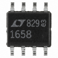
LTC1658CS8#PBF Linear Technology, LTC1658CS8#PBF Datasheet - Page 5

LTC1658CS8#PBF
Manufacturer Part Number
LTC1658CS8#PBF
Description
IC D/A CONV 14BIT R-R 8-SOIC
Manufacturer
Linear Technology
Datasheet
1.LTC1658CS8PBF.pdf
(12 pages)
Specifications of LTC1658CS8#PBF
Settling Time
12µs
Number Of Bits
14
Data Interface
Serial
Number Of Converters
1
Voltage Supply Source
Single Supply
Power Dissipation (max)
3mW
Operating Temperature
0°C ~ 70°C
Mounting Type
Surface Mount
Package / Case
8-SOIC (3.9mm Width)
Number Of Channels
1
Resolution
14b
Interface Type
Serial (3-Wire, SPI, Microwire)
Single Supply Voltage (typ)
3/5V
Dual Supply Voltage (typ)
Not RequiredV
Power Supply Requirement
Single
Output Type
Voltage
Integral Nonlinearity Error
±8LSB
Single Supply Voltage (min)
2.7V
Single Supply Voltage (max)
5.5V
Dual Supply Voltage (min)
Not RequiredV
Dual Supply Voltage (max)
Not RequiredV
Operating Temp Range
0C to 70C
Operating Temperature Classification
Commercial
Mounting
Surface Mount
Pin Count
8
Package Type
SOIC N
Lead Free Status / RoHS Status
Lead free / RoHS Compliant
Available stocks
Company
Part Number
Manufacturer
Quantity
Price
TYPICAL PERFOR A CE CHARACTERISTICS
CLK (Pin 1): The TTL Level Input for the Serial Interface
Clock.
D
Data. Data on the D
on the rising edge of the serial clock and is loaded MSB
first. The LTC1658 requires a 16-bit word to be loaded in.
The last two bits are don’t cares.
CS/LD (Pin 3): The TTL Level Input for the Serial Inter-
face Enable and Load Control. When CS/LD is low the
CLK signal is enabled, so the data can be clocked in.
When CS/LD is pulled high, data is loaded from the shift
register into the DAC register, updating the DAC output.
PIN
IN
U
(Pin 2): The TTL Level Input for the Serial Interface
FUNCTIONS
U
–1
–2
–3
–4
–5
5
4
3
2
1
0
–55
Gain Error vs Temperature
IN
–25
U
pin is latched into the shift register
TEMPERATURE ( C)
5
W
35
U
65
95
1658 G06
125
D
Valid on the Rising Edge of the Serial Clock.
GND (Pin 5): Ground.
REF (Pin 6): Reference Input. There is a gain of one from
this pin to the output. When tied to V
swing from GND to V
within it’s offset specification of V
Information).
V
V
OUT
CC
OUT
(Pin 8): Positive Supply Input. 2.7V V
(Pin 4): Output of the Shift Register Which Becomes
(Pin 7): Buffered Rail-to-Rail DAC Output.
1LSB/DIV
Broadband Noise
BW = 1Hz TO
100kHz
CC
. The output can only swing to
200 s/DIV
CC
CC
(see Applicatons
1658 G08
LTC1658
the output will
CC
5.5V.
5


