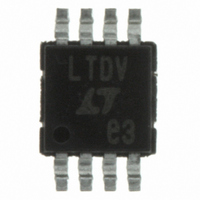
LTC1661CMS8#PBF Linear Technology, LTC1661CMS8#PBF Datasheet - Page 3

LTC1661CMS8#PBF
Manufacturer Part Number
LTC1661CMS8#PBF
Description
IC D/A CONV 10BIT MICRPWR 8-MSOP
Manufacturer
Linear Technology
Datasheet
1.LTC1661CMS8PBF.pdf
(14 pages)
Specifications of LTC1661CMS8#PBF
Settling Time
30µs
Number Of Bits
10
Data Interface
Serial
Number Of Converters
2
Voltage Supply Source
Single Supply
Power Dissipation (max)
260µW
Operating Temperature
0°C ~ 70°C
Mounting Type
Surface Mount
Package / Case
8-MSOP, Micro8™, 8-uMAX, 8-uSOP,
Lead Free Status / RoHS Status
Lead free / RoHS Compliant
Available stocks
Company
Part Number
Manufacturer
Quantity
Price
ELECTRICAL CHARACTERISTICS
TIMING CHARACTERISTICS
temperature range, otherwise specifications are at T
range, otherwise specifications are at T
SYMBOL
V
t
t
t
t
t
t
t
t
t
SYMBOL
Reference Input
I
Power Supply
V
I
DC Performance
AC Performance
Digital I/O
V
V
I
C
1
2
3
4
5
6
7
9
11
REF
CC
LK
CC
CC
IH
IL
IN
= 4.5V to 5.5V
PARAMETER
Input Voltage Range
Resistance
Capacitance
Reference Current
Positive Supply Voltage
Supply Current
Short-Circuit Current Low
Short-Circuit Current High
Voltage Output Slew Rate
Voltage Output Settling Time
Capacitive Load Driving
Digital Input High Voltage
Digital Input Low Voltage
Digital Input Leakage
Digital Input Capacitance
PARAMETER
D
D
SCK High Time
SCK Low Time
CS/LD Pulse Width
LSB SCK High to CS/LD High
CS/LD Low to SCK High
SCK Low to CS/LD Low
CS/LD High to SCK Positive Edge
SCK Frequency
IN
IN
Valid to SCK Setup
Valid to SCK Hold
A
= 25°C.
CONDITIONS
Active Mode
Sleep Mode
For Specified Performance
V
V
Sleep Mode (Note 3)
V
V
Rising (Notes 4, 5)
Falling (Notes 4, 5)
To ±0.5LSB (Notes 4, 5)
V
V
V
V
V
(Note 6)
CONDITIONS
(Note 6)
(Note 6)
(Note 6)
(Note 6)
(Note 6)
(Note 6)
(Note 6)
Square Wave (Note 6)
CC
CC
OUT
OUT
CC
CC
CC
CC
IN
The
= GND to V
A
= 5V (Note 3)
= 5V (Note 3)
= 2.7V to 5.5V
= 2.7V to 3.6V
= 4.5V to 5.5V
= 2.7V to 5.5V
= 0V, V
= V
= 25°C. V
l
CC
denotes the specifications which apply over the full operating temperature
The
= V
CC
REF
CC
= V
l
CC
REF
denotes the specifications which apply over the full operating
= 5V, Code = 0
= 2.7V to 5.5V, V
= 5V, Code = 1023
REF
≤ V
CC
l
l
l
l
l
l
l
l
l
l
l
l
l
l
l
l
l
l
l
l
l
l
l
l
l
l
, V
OUT
MIN
140
2.7
2.4
2.0
10
MIN
0
7
40
30
30
80
30
20
20
unloaded unless otherwise noted.
0
0
0.001
1000
0.60
0.25
TYP
260
120
TYP
15
95
25
19
30
1
LTC1661
MAX
MAX
V
195
154
100
120
±10
16.7
5.5
0.8
0.6
10
1
3
CC
UNITS
UNITS
1661fa
3
V/µs
V/µs
MHz
mA
mA
kΩ
µA
µA
µA
µA
µA
pF
µs
pF
pF
ns
ns
ns
ns
ns
ns
ns
ns
ns
V
V
V
V
V
V


