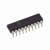
X9221UP Intersil, X9221UP Datasheet - Page 4

X9221UP
Manufacturer Part Number
X9221UP
Description
IC DCP DUAL 50K 64TP 20DIP
Manufacturer
Intersil
Series
XDCP™r
Datasheet
1.X9221UP.pdf
(15 pages)
Specifications of X9221UP
Taps
64
Resistance (ohms)
50K
Number Of Circuits
2
Temperature Coefficient
30 ppm/°C Typical
Memory Type
Non-Volatile
Interface
I²C, 2-Wire Serial
Voltage - Supply
4.5 V ~ 5.5 V
Operating Temperature
0°C ~ 70°C
Mounting Type
Through Hole
Package / Case
20-DIP (0.300", 7.62mm)
Resistance In Ohms
50K
Lead Free Status / RoHS Status
Contains lead / RoHS non-compliant
Available stocks
Company
Part Number
Manufacturer
Quantity
Price
Company:
Part Number:
X9221UP
Manufacturer:
Intersil
Quantity:
2 150
Part Number:
X9221UP
Manufacturer:
WOLFSON
Quantity:
20 000
X9221
Instruction Structure
The next byte sent to the X9221 contains the instruc-
tion and register pointer information. The four most
significant bits are the instruction. The next four bits
point to one of two pots and when applicable they
point to one of four associated registers. The format is
shown below in Figure 2.
Figure 2. Instruction Byte Format
t
The four high order bits define the instruction. The
sixth bit (P0) selects which one of the two potentiome-
ters is to be affected by the instruction. The last two
bits (R1 and R0) select one of the four registers that is
to be acted upon when a register oriented instruction
is issued.
Four of the nine instructions end with the transmission
of the instruction byte. The basic sequence is illus-
trated in Figure 3. These two-byte instructions
exchange data between the WCR and one of the data
registers. A transfer from a data register to a WCR is
essentially a write to a static RAM. The response of
REV 1.1 8/8/02
Figure 3. Two-Byte Command Sequence
I3
SDA
SCL
Instructions
I2
I1
S
A
R
T
T
I0
0
1
Potentiometer
0
Select
0
P0
1
R1
Register
A3 A2 A1 A0
Select
R0
www.xicor.com
A
C
K
the wiper to this action will be delayed t
fer from WCR’s current wiper position to a data regis-
ter is a write to nonvolatile memory and takes a
minimum of t
between either potentiometer and their associated
registers or it may occur between both of the potenti-
ometers and one of their associated registers.
Four instructions require a three-byte sequence to
complete. These instructions transfer data between
the host and the X9221; either between the host and
one of the data registers or directly between the host
and the WCR. These instructions are: Read WCR,
read the current wiper position of the selected pot;
Write WCR, change current wiper position of the
selected pot; Read Data Register, read the contents of
the selected nonvolatile register; Write Data Register,
write a new value to the selected data register. The
sequence of operations is shown in Figure 4.
The Increment/Decrement command is different from
the other commands. Once the command is issued
and the X9221 has responded with an acknowledge,
the master can clock the selected wiper up and/or
down in one segment steps; thereby, providing a fine
tuning capability to the host. For each SCL clock pulse
(t
move one resistor segment towards the V
nal. Similarly, for each SCL clock pulse while SDA is
LOW, the selected wiper will move one resistor seg-
ment towards the V
of the sequence and timing for this operation are
shown in Figures 5 and 6 respectively.
I3
HIGH
I2
) while SDA is HIGH, the selected wiper will
I1
I0
WR
0
to complete. The transfer can occur
Characteristics subject to change without notice.
L
/R
P0 R1 R0
L
terminal. A detailed illustration
C
A
K
S
O
P
T
STPWV
H
/R
. A trans-
H
termi-
4 of 15


