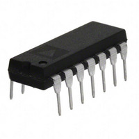
AD7376AN100 Analog Devices Inc, AD7376AN100 Datasheet - Page 8

AD7376AN100
Manufacturer Part Number
AD7376AN100
Description
IC DIGITAL POT 14-DIP
Manufacturer
Analog Devices Inc
Specifications of AD7376AN100
Rohs Status
RoHS non-compliant
Taps
128
Resistance (ohms)
100K
Number Of Circuits
1
Temperature Coefficient
300 ppm/°C Typical
Memory Type
Volatile
Interface
SPI, 3-Wire Serial
Voltage - Supply
4.5 V ~ 33 V, ±4.5 V ~ 16.5 V
Operating Temperature
-40°C ~ 85°C
Mounting Type
Through Hole
Package / Case
14-DIP (0.300", 7.62mm)
Resistance In Ohms
100K
Number Of Elements
1
# Of Taps
128
Resistance (max)
100KOhm
Power Supply Requirement
Single/Dual
Interface Type
Serial (3-Wire/SPI)
Single Supply Voltage (typ)
5/9/12/15/18/24V
Dual Supply Voltage (typ)
±5/±15V
Single Supply Voltage (min)
4.5V
Single Supply Voltage (max)
28V
Dual Supply Voltage (min)
±4.5V
Dual Supply Voltage (max)
±16.5V
Operating Temp Range
-40C to 85C
Operating Temperature Classification
Industrial
Mounting
Through Hole
Pin Count
14
Lead Free Status / RoHS Status
Not Compliant
AD7376
OPERATION
The AD7376 provides a 128-position digitally-controlled vari-
able resistor (VR) device. Changing the programmed VR set-
tings is accomplished by clocking in a 7-bit serial data word into
the SDI (Serial Data Input) pin, while CS is active low. When
CS returns high the last seven bits are transferred into the RDAC
latch setting the new wiper position. The exact timing require-
ments are shown in Figure 1.
The AD7376 resets to a midscale by asserting the RS pin, sim-
plifying initial conditions at power-up. Both parts have a power
shutdown SHDN pin which places the RDAC in a zero power
consumption state where terminal A is open circuited and the
wiper W is connected to B, resulting in only leakage currents
being consumed in the VR structure. In shutdown mode the
VR latch settings are maintained so that, returning to opera-
tional mode from power shutdown, the VR settings return to
their previous resistance values.
Figure 39. Common-Mode Leakage Current Test Circuit
Figure 38. Incremental ON Resistance Test Circuit
Figure 40. AD7376 Equivalent RDAC Circuit
SHDN
DUT
D 6
D 5
D 4
D 3
D 2
D 1
D 0
DECODER
V
V
DUT
LATCH
RDAC
DD
SS
B
&
W
GND
R
NC
NC
S
R
R
R
R
A
B
S
S
S
S
= R
I
SW
W
NOMINAL
V
CODE = OO
SS
R
SW
TO V
I
CM
/128
=
V
0.1V
I
CM
DD
SW
H
0.1V
W
B
A
–8–
PROGRAMMING THE VARIABLE RESISTOR
Rheostat Operation
The nominal resistance of the RDAC between terminals A and
B are available with values of 10 k , 50 k , 100 k and 1 M .
The final three characters of the part number determine the
nominal resistance value, e.g., 10 k = 10; 50 k = 50; 100 k
= 100; 1 M = 1M. The nominal resistance (R
has 128 contact points accessed by the wiper terminal, plus the
B terminal contact. The 7-bit data word in the RDAC latch is
decoded to select one of the 128 possible settings. The wiper’s first
connection starts at the B terminal for data 00
nal connection has a wiper contact resistance of 120 . The
second connection (10 k part) is the first tap point located
at 198
for data 01
senting 156 + 120 = 276
increase moves the wiper up the resistor ladder until the last tap
point is reached at 10041 . The wiper does not directly con-
nect to the B terminal. See Figure 40 for a simplified diagram of
the equivalent RDAC circuit.
The general transfer equation that determines the digitally pro-
grammed output resistance between W and B is:
where D is the data contained in the 7-bit VR latch, and R
the nominal end-to-end resistance.
For example, when V
following output resistance values will be set for the following
VR latch codes (applies to the 10 k potentiometer).
D
(DEC)
127
64
1
0
Note that in the zero-scale condition a finite wiper resistance of
120
between W and B in this state to a maximum value of 5 mA to
avoid degradation or possible destruction of the internal switch
contact.
Like the mechanical potentiometer the RDAC replaces, it is
totally symmetrical. The resistance between the wiper W and
terminal A also produces a digitally controlled resistance R
When these terminals are used the B–terminal should be tied to
the wiper. Setting the resistance value for R
mum value of resistance and decreases as the data loaded in the
latch is increased in value. The general transfer equation for this
operation is:
where D is the data contained in the 7-bit RDAC latch, and R
is the nominal end-to-end resistance. For example, when V
and B–terminal is tied to the wiper W the following output
resistance values will be set for the following RDAC latch codes.
R
R
WB
WA
is present. Care should be taken to limit the current flow
(D) = (D)/128
(= R
(D) = (128-D)/128
H
R
( )
10041
5120
276
198
. The third connection is the next tap point repre-
WB
BA
[nominal resistance]/128 + R
B
= 0 V and A–terminal is open circuit, the
Output State
Full-Scale
Midscale (RS = 0 Condition)
1 LSB
Zero-Scale (Wiper Contact Resistance)
R
BA
for data 02
Table I.
+ R
R
BA
W
+ R
H
W
. Each LSB data value
WA
W
H
= 78
starts at a maxi-
AB
. This B–termi-
) of the VR
+ 120 )
A
REV. 0
= 0 V
BA
WA
is
.
(2)
(1)
BA


