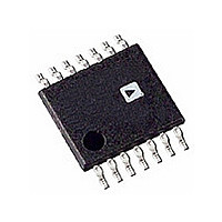
AD5260BRU20-REEL7 Analog Devices Inc, AD5260BRU20-REEL7 Datasheet - Page 4

AD5260BRU20-REEL7
Manufacturer Part Number
AD5260BRU20-REEL7
Description
IC DGTL POT SNGL 256POS 14-TSSOP
Manufacturer
Analog Devices Inc
Specifications of AD5260BRU20-REEL7
Rohs Status
RoHS non-compliant
Taps
256
Resistance (ohms)
20K
Number Of Circuits
1
Temperature Coefficient
35 ppm/°C Typical
Memory Type
Volatile
Interface
4-Wire SPI Serial
Voltage - Supply
4.5 V ~ 16.5 V, ±4.5 V ~ 5.5 V
Operating Temperature
-40°C ~ 85°C
Mounting Type
Surface Mount
Package / Case
14-TSSOP
Resistance In Ohms
20K
Number Of Elements
1
# Of Taps
256
Resistance (max)
20KOhm
Power Supply Requirement
Single/Dual
Interface Type
Serial (4-Wire/SPI)
Single Supply Voltage (typ)
15V
Dual Supply Voltage (typ)
±5V
Single Supply Voltage (min)
4.5V
Single Supply Voltage (max)
16.5V
Dual Supply Voltage (min)
±4.5V
Dual Supply Voltage (max)
±5.5V
Operating Temp Range
-40C to 85C
Operating Temperature Classification
Industrial
Mounting
Surface Mount
Pin Count
14
Lead Free Status / RoHS Status
Not Compliant
AD5260/AD5262
Parameter
DYNAMIC CHARACTERISTICS
INTERFACE TIMING CHARACTERISTICS
1
2
3
4
5
6
7
8
9
10
11
12
13
Typical values represent average readings at 25°C and V
Resistor position nonlinearity error (R-INL) is the deviation from an ideal value measured between the maximum resistance and the minimum resistance wiper
positions. R-DNL measures the relative step change from ideal between successive tap positions. Parts are guaranteed monotonic. I
V
V
INL and DNL are measured at V
DNL specification limits of ±1 LSB maximum are guaranteed monotonic operating conditions.
Resistor Terminal A, Terminal B, and Terminal W have no limitations on polarity with respect to each other.
Guaranteed by design and not subject to production test.
Measured at the Ax terminals. All Ax terminals are open-circuit in shutdown mode.
Worst-case supply current consumed when all logic-input levels set at 2.4 V, which is the standard characteristic of CMOS logic.
P
Switching characteristics are measured using V
All dynamic characteristics use V
Measured at V
See Figure 5 for location of measured values. All input control voltages are specified with t
Propagation delay depends on value of V
SS
AB
DISS
Bandwidth –3 dB
Total Harmonic Distortion
V
Crosstalk
Analog Crosstalk
Resistor Noise Voltage
Clock Frequency
Input Clock Pulse Width
Data Setup Time
Data Hold Time
CLK to SDO Propagation Delay
CS Setup Time
CS High Pulse Width
Reset Pulse Width
CLK Fall to CS Rise Hold Time
CS Rise to Clock Rise Setup
W
= −5V.
= V
is calculated from (I
Settling Time
DD
, wiper = no connect.
11
W
where an adjacent V
DD
× V
DD
W
6, 10
). CMOS logic level inputs result in minimum power dissipation.
with the RDAC configured as a potentiometer divider similar to a voltage output digital-to-analog converter. V
DD
= +5 V, V
13
W
is making a full-scale voltage change.
6, 12
DD
, R
SS
L
= −5 V, V
L
, and C
= 5 V.
L
.
L
DD
= +5 V.
= +5 V, V
Symbol
BW
THD
t
C
C
e
f
t
t
t
t
t
t
t
t
t
CLK
S
CH
DS
DH
PD
CSS
CSW
RS
CSH
CS1
N_WB
T
TA
SS
, t
= −5 V.
W
CL
Rev. A | Page 4 of 24
Conditions
R
V
R
V
error band, R
V
with adjacent RDAC making
full-scale code change (AD5262
only)
V
with V
R
only)
R
Specifications apply to all parts
Clock level high or low
R
AB
AB
AB
WB
L
A
A
A
A1
= 1 kΩ, C
= 1 V
= +5 V, V
= V
= 20 kΩ/50 kΩ/200 kΩ
= 20 kΩ
= V
= 20 kΩ/200 kΩ (AD5262
= 20 kΩ, f = 1 kHz
DD
W2
DD
RMS
, V
R
, V
= 5 V p-p at f = 10 kHz,
= t
, V
B
B1
B
= 0 V, measure V
L
F
< 20 pF
B
= −5 V, ±1 LSB
= 2 ns (10% to 90% of 3 V) and timed from a voltage level of 1.5 V.
AB
= 0 V, measure V
= 0 V, f = 1 kHz,
= 20 kΩ
W
W1
Min
20
10
10
1
5
20
50
0
10
Typ
310/130/30
0.014
5
1
–64
13
W
= V
1
DD
/R for both V
A
= V
Max
25
160
DD
and V
DD
= +5 V and
B
Unit
kHz
%
μs
nV-sec
dB
nV/√Hz
MHz
ns
ns
ns
ns
ns
ns
ns
ns
ns
= 0 V.


