AD5222BR10-REEL7 Analog Devices Inc, AD5222BR10-REEL7 Datasheet - Page 2
AD5222BR10-REEL7
Manufacturer Part Number
AD5222BR10-REEL7
Description
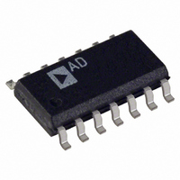
IC DGTL POT DUAL 128POS 14-SOIC
Manufacturer
Analog Devices Inc
Datasheet
1.AD5222BRUZ10-REEL7.pdf
(10 pages)
Specifications of AD5222BR10-REEL7
Rohs Status
RoHS non-compliant
Taps
128
Resistance (ohms)
10K
Number Of Circuits
2
Temperature Coefficient
35 ppm/°C Typical
Memory Type
Volatile
Interface
Up/Down Counter
Voltage - Supply
2.7 V ~ 5.5 V, ±2.3 V ~ 2.7 V
Operating Temperature
-40°C ~ 85°C
Mounting Type
Surface Mount
Package / Case
14-SOIC (3.9mm Width), 14-SOL
Resistance In Ohms
10K


Parameter
DC CHARACTERISTICS RHEOSTAT MODE (Specifications Apply to All VRs)
DC CHARACTERISTICS POTENTIOMETER DIVIDER MODE (Specifications Apply to All VRs)
RESISTOR TERMINALS
DIGITAL INPUTS AND OUTPUTS
POWER SUPPLIES
DYNAMIC CHARACTERISTICS
INTERFACE TIMING CHARACTERISTICS (Applies to All Parts)
NOTES
10
Specifications subject to change without notice.
AD5222–SPECIFICATIONS
1
2
3
4
5
6
7
8
9
Typicals represent average readings at 25 C, V
Resistor position nonlinearity error R-INL is the deviation from an ideal value measured between the maximum resistance and the minimum resistance wiper positions.
Wiper resistance is not measured on the R
INL and DNL are measured at V
Resistor Terminals A, B, W have no limitations on polarity with respect to each other.
Guaranteed by design and not subject to production test.
P
Bandwidth, noise and settling time are dependent on the terminal resistance value chosen. The lowest R value results in the fastest settling time and highest bandwidth.
All dynamic characteristics use V
See timing diagram for location of measured values. All input control voltages are specified with t
R-DNL measures the relative step change from ideal between successive tap positions. Parts are guaranteed monotonic. See Figure 22 test circuit.
specification limits of 1 LSB maximum are guaranteed monotonic operating conditions. See Figure 21 test circuit.
The highest R value results in the minimum overall power consumption.
of 1.5 V. Switching characteristics are measured using both V
Resistor Differential NL
Resistor Nonlinearity
Nominal Resistor Tolerance
Resistance Temperature Coefficient
Wiper Resistance
Nominal Resistance Match
Resolution
Integral Nonlinearity
Differential Nonlinearity
Voltage Divider Temperature Coefficient
Full-Scale Error
Zero-Scale Error
Voltage Range
Capacitance
Capacitance
Common-Mode Leakage
Input Logic High
Input Logic Low
Input Current
Input Capacitance
Power Single-Supply Range
Power Dual-Supply Range
Positive Supply Current
Negative Supply Current
Power Dissipation
Power Supply Sensitivity
Bandwidth –3 dB
Total Harmonic Distortion
V
Resistor Noise Voltage
Input Clock Pulsewidth
CS to CLK Setup Time
CS Rise to CLK Hold Time
U/D to Clock Fall Setup Time
U/D to Clock Fall Hold Time
DACSEL to Clock Fall Setup Time
DACSEL to Clock Fall Hold Time
MODE to Clock Fall Setup Time
MODE to Clock Fall Hold Time
DISS
W
Settling Time
is calculated from (I
6
6
A, B
W
5
3
7
6
DD
4
2
2
4
V
DD
DD
W
). CMOS logic level inputs result in minimum power dissipation.
with the RDAC configured as a potentiometer divider similar to a voltage output D/A converter. V
= 5 V.
6, 8, 9
AB
= 1 M models.
DD
= 5 V.
Symbol
R-DNL
R-INL
R
R
N
INL
INL
DNL
V
V
V
C
C
I
V
V
I
C
V
V
I
I
P
PSS
BW_10K
BW_50K
BW_100K
BW_1M
THD
t
e
t
t
t
t
t
t
t
t
t
CM
IL
DD
SS
S
CH
CSS
CSH
UDS
UDH
DSS
DSH
MDS
MDH
N_WB
R
R/R
V
DISS
AB
W
WFSE
WZSE
A, B, W
A, B
W
IH
IL
IL
DD RANGE
DD/SS RANGE
W
, t
/ T
/ T
O
CL
W
DD
(V
unless otherwise noted.)
= 5 V or V
DD
= 3 V
Condition
R
R
V
V
I
CH 1 to 2, V
R
R
Code = 40
Code = 7F
Code = 00
f = 1 MHz, Measured to GND, Code = 40
f = 1 MHz, Measured to GND, Code = 40
V
V
V
V
V
V
V
V
R
R
R
R
V
R
R
Clock Level High or Low
W
WB
WB
AB
AB
AB
AB
A
DD
DD
IN
SS
IH
SS
IH
AB
AB
AB
AB
A
AB
WB
= V
= 1 V rms + 2 V dc, V
= V
= 0 V
= –2.5 V, V
, V
, V
= V
= V
= 10 k , 50 k , or 100 k
= 1 M
= 0 V or 5 V
= 5 V or V
= 5 V or V
= 10 k , Code = 40
= 50 k , Code = 40
= 100 k , Code = 40
= 500 k , Code = 40
= 10 k , 1 LSB Error Band
DD
= 5 V/3 V
= 5 V/3 V
= 5 k , f = 1 kHz
DD
A
A
B
= 3 V.
–2–
10% or 5 V
DD
DD
= NC
= NC
= V
/R, V
6, 10
, Wiper = No Connect, T
, Wiper = No Connect
H
H
H
W
AB
DD
IL
IL
DD
= V
= 0 V
= 0 V, V
= 3 V or 5 V
= +2.7 V
DD
10%, V
, T
R
= t
B
H
H
A
DD
H
H
= 2 V dc, f = 1 kHz
F
= 25 C
= 2.5 ns (10% to 90% of +3 V) and timed from a voltage level
= 5 V
SS
= 0 V, V
A
= 25 C
A
= +V
H
H
DD
, V
Min
–1
–1
–30
7
–1
–2
–1
–1
0
V
2.4/2.1
2.7
30
20
20
10
30
20
30
20
40
2.3
SS
B
= 0 V, –40 C < T
A
= V
Typ
–35
45
0.2
20
–0.5 +0
0.5
45
60
1
5
15
15
150
0.002 0.05
1000
180
78
7
0.005
2
14
1/4 +1
0.4 +1
1/4 +1
1/2 +2
1/4 +1
DD
1
and V
Max
+30
100
1
1
V
0.8/0.6 V
5.5
40
40
400
1
2.7
DD
B
= 0 V. DNL
A
< +85 C,
Unit
LSB
LSB
%
ppm/ C
%
Bits
LSB
LSB
LSB
ppm/ C
LSB
LSB
V
pF
pF
nA
V
pF
V
V
%/%
kHz
kHz
kHz
kHz
%
nV Hz
ns
ns
ns
ns
ns
ns
ns
ns
ns
REV. 0
A
A
A
W
s
Related parts for AD5222BR10-REEL7
Image
Part Number
Description
Manufacturer
Datasheet
Request
R

Part Number:
Description:
IC DGTL POT DUAL 128POS 14-SOIC
Manufacturer:
Analog Devices Inc
Datasheet:

Part Number:
Description:
±1.7g Dual-Axis IMEMS Accelerometer Evaluation Board
Manufacturer:
Analog Devices Inc
Datasheet:

Part Number:
Description:
Inertial Sensor Evaluation System
Manufacturer:
Analog Devices Inc
Datasheet:
Part Number:
Description:
Manufacturer:
Analog Devices Inc
Datasheet:
Part Number:
Description:
Manufacturer:
Analog Devices Inc
Datasheet:
Part Number:
Description:
Manufacturer:
Analog Devices Inc
Datasheet:
Part Number:
Description:
Manufacturer:
Analog Devices Inc
Datasheet:
Part Number:
Description:
Manufacturer:
Analog Devices Inc
Datasheet:
Part Number:
Description:
Manufacturer:
Analog Devices Inc
Datasheet:
Part Number:
Description:
Manufacturer:
Analog Devices Inc
Datasheet:
Part Number:
Description:
Manufacturer:
Analog Devices Inc
Datasheet:
Part Number:
Description:
Manufacturer:
Analog Devices Inc
Datasheet:
Part Number:
Description:
Manufacturer:
Analog Devices Inc
Datasheet: