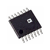
AD5280BRU200 Analog Devices Inc, AD5280BRU200 Datasheet - Page 17

AD5280BRU200
Manufacturer Part Number
AD5280BRU200
Description
IC DGTL POT 200K 256POS 14-TSSOP
Manufacturer
Analog Devices Inc
Datasheet
1.AD5280BRUZ50.pdf
(28 pages)
Specifications of AD5280BRU200
Rohs Status
RoHS non-compliant
Taps
256
Resistance (ohms)
200K
Number Of Circuits
1
Temperature Coefficient
30 ppm/°C Typical
Memory Type
Volatile
Interface
I²C, 2-Wire Serial
Voltage - Supply
4.5 V ~ 16.5 V, ±4.5 V ~ 5.5 V
Operating Temperature
-40°C ~ 85°C
Mounting Type
Surface Mount
Package / Case
14-TSSOP
Resistance In Ohms
200K
Number Of Elements
1
# Of Taps
256
Resistance (max)
200KOhm
Power Supply Requirement
Single/Dual
Interface Type
Serial (2-Wire/I2C)
Single Supply Voltage (typ)
15V
Dual Supply Voltage (typ)
±5V
Single Supply Voltage (min)
4.5V
Single Supply Voltage (max)
16.5V
Dual Supply Voltage (min)
±4.5V
Dual Supply Voltage (max)
±5.5V
Operating Temp Range
-40C to 85C
Operating Temperature Classification
Industrial
Mounting
Surface Mount
Pin Count
14
Lead Free Status / RoHS Status
Not Compliant
READBACK RDAC VALUE
The AD5280/AD5282 allow the user to read back the RDAC
values in read mode. However, for the dual-channel AD5282,
the channel of interest is the one that is previously selected in
the write mode. When users need to read the RDAC values of
both channels in the AD5282, they can program the first
subaddress in write mode and then change to read mode to read
the first channel value. After that, they can change back to write
mode with the second subaddress and read the second channel
value in read mode again. It is not necessary for users to issue
the Frame 3 data byte in write mode for subsequent readback
operation. Users should refer to Figure 45 and Figure 46 for the
programming format.
ADDITIONAL PROGRAMMABLE LOGIC OUTPUT
The AD5280/AD5282 feature additional programmable logic
outputs, O
analog switches, and logic gates. O
logic states of O
write mode (see Figure 45). These logic outputs have adequate
current driving capability to sink/source milliamperes of load.
Users can also activate O
affecting the wiper settings by programming as follows:
•
•
•
SELF-CONTAINED SHUTDOWN FUNCTION AND
PROGRAMMABLE PRESET
Shutdown can be activated by strobing the SHDN pin or
programming the SD bit in the write mode instruction byte.
As shown in
AD5280/AD5282 open SW
short the W terminal to the B terminal. The AD5280/AD5282
consume negligible power during shutdown mode, resuming
the previous setting once the
Perform start, slave address, acknowledge, and instruction
bytes with O
Complete the write cycle with stop, then start, slave address
byte, acknowledge, instruction byte with O
specified, acknowledge, stop.
Not complete the write cycle by not issuing the stop, then
start, slave address byte, acknowledge, instruction byte
with O
1
and O
1
and O
Figure 44
1
and O
1
2
, which can be used to drive a digital load,
and O
2
specified, acknowledge, stop.
, when shutdown is asserted, the
2
can be programmed in Frame 2 under
1
2
and O
specified, acknowledge, stop.
A
to let the A terminal float and
SHDN pin is released.
2
1
in three ways without
and O
2
default to Logic 0. The
1
and O
2
Rev. C | Page 17 of 28
In addition, shutdown can be implemented with the device
digital output as shown in Figure 47. In this configuration, the
device is shut down during power-up, but the user is allowed to
program the device at any preset levels. When it is done, the
user programs O
exits from shutdown and responds to the new setting. This self-
contained shutdown function allows absolute shutdown during
power-up, which is crucial in hazardous environments, without
adding extra components. Also, the sleep mode programming
feature during shutdown allows the AD5280/AD5282 to have a
programmable preset at any level, a solution that can be as
effective as using other high cost EEPROM devices. Because of
the extra power drawn on R
chosen for the R
MULTIPLE DEVICES ON ONE BUS
Figure 48 shows four AD5282 devices on the same serial bus.
Each has a different slave address because the states of their Pin
AD0 and Pin AD1 are different. This allows each RDAC within
each device to be written to or read from independently. The
master device output bus line drivers are open-drain pull-
downs in a fully I
MASTER
SDA
AD5282
AD1
AD0
Figure 48. Multiple AD5282 Devices on One Bus
Figure 47. Shutdown by Internal Logic Output
SCL
PD
1
2
R
high with the valid coding and the device
C-compatible interface.
.
P
5V
R
P
R
AD5282
SDA
PD
AD1
AD0
5V
PD
SCL
, note that a high value should be
SDA
SCL
O
SHDN
1
5V
AD5280/AD5282
AD5282
SDA
AD1
AD0
SCL
5V
AD5282
SDA
AD1
AD0
SCL
SDA
SCL


