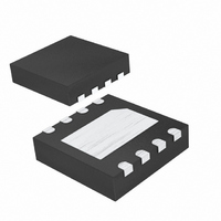
MAX5424ETA+T Maxim Integrated Products, MAX5424ETA+T Datasheet - Page 7

MAX5424ETA+T
Manufacturer Part Number
MAX5424ETA+T
Description
IC POT DGTL 256-TAP NV 8-TDFN
Manufacturer
Maxim Integrated Products
Datasheet
1.MAX5423ETAT.pdf
(11 pages)
Specifications of MAX5424ETA+T
Package / Case
8-TDFN Exposed Pad
Mounting Type
Surface Mount
Voltage - Supply
2.7 V ~ 5.25 V
Operating Temperature
-40°C ~ 85°C
Temperature Coefficient
35 ppm/°C Typical
Interface
SPI, 3-Wire Serial
Resistance In Ohms
200K
Number Of Circuits
1
Memory Type
Non-Volatile
Taps
256
Number Of Pots
Single
Taps Per Pot
256
Resistance
200 KOhms
Wiper Memory
Non Volatile
Digital Interface
Serial (3-Wire, SPI)
Operating Supply Voltage
5 V
Supply Current
0.001 mA
Maximum Operating Temperature
+ 85 C
Minimum Operating Temperature
- 40 C
Description/function
200kOhm, 256-Tap, Nonvolatile, SPI-Interface Digital Potentiometer
Mounting Style
SMD/SMT
Supply Voltage (max)
5.25 V
Supply Voltage (min)
2.7 V
Tolerance
25 %
Lead Free Status / RoHS Status
Lead free / RoHS Compliant
Figure 1. Digital Interface and Timing Diagram
The MAX5422/MAX5423/MAX5424 contain a resistor
array with 255 resistive elements. The MAX5422 has a
total end-to-end resistance of 50kΩ; the MAX5423 has
an end-to-end resistance of 100kΩ; and the MAX5424
has an end-to-end resistance of 200kΩ. The
MAX5422/MAX5423/MAX5424 allow access to the high,
low, and wiper terminals for a standard voltage-divider
configuration. H, L, and W can be connected in any
desired configuration as long as their voltages fall
between GND and V
A simple, 3-wire, SPI serial interface moves the wiper
among the 256 tap points. The nonvolatile memory
stores the wiper position and recalls the stored wiper
position upon power-up. The nonvolatile memory is
guaranteed for 50 years for wiper data retention and up
to 200,000 wiper store cycles.
PIN
—
1
2
3
4
5
6
7
8
SCLK
DIN
CS
NAME
SCLK
GND
V
DIN
CS
EP
W
DD
H
L
_______________________________________________________________________________________
t
DD
CS0
Power-Supply Input. Bypass V
Serial-Interface Clock Input
Serial-Interface Data Input
Active-Low Digital-Input Chip Select
Ground
Low Terminal. The voltage at L can be greater than or less than the voltage at H. Current can flow into or
out of L.
Wiper Terminal
High Terminal. The voltage at H can be greater than or less than the voltage at L. Current can flow into or
out of H.
Exposed Pad. The exposed pad is not internally connected. Connect to GND or leave floating.
Detailed Description
.
t
CSS
256-Tap, Nonvolatile, SPI-Interface,
t
DS
t
CL
t
DD
DH
t
CH
with a 0.1µF capacitor from V
The MAX5422/MAX5423/MAX5424 consist of a resistor
array with 255 resistive elements; 256 tap points are
accessible to the wiper, W, along the resistor string
between H and L. Select the wiper tap point by pro-
gramming the potentiometer through the 3-wire (SPI)
interface. Eight data bits, and a control byte program
the wiper position. The H and L terminals of the
MAX5422/MAX5423/MAX5424 are similar to the two
end terminals of a mechanical potentiometer. The
MAX5422/MAX5423/MAX5424 feature power-on reset
circuitry that loads the wiper position from the non-
volatile memory at power-up.
The MAX5422/MAX5423/MAX5424 use a 3-wire, SPI-
compatible, serial data interface (Figure 1 and 2). This
write-only interface contains three inputs: chip-select
Digital Potentiometers
FUNCTION
t
CP
DD
to GND.
t
CSH
Pin Description
Digital Interface
Analog Circuitry
t
CSW
t
CS1
7


