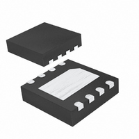
MAX5419LETA+T Maxim Integrated Products, MAX5419LETA+T Datasheet - Page 4

MAX5419LETA+T
Manufacturer Part Number
MAX5419LETA+T
Description
IC POT DGTL 256-TAP I2C 8-TDFN
Manufacturer
Maxim Integrated Products
Specifications of MAX5419LETA+T
Package / Case
8-TDFN Exposed Pad
Mounting Type
Surface Mount
Voltage - Supply
2.7 V ~ 5.25 V
Operating Temperature
-40°C ~ 85°C
Temperature Coefficient
35 ppm/°C Typical
Interface
I²C, 2-Wire Serial
Resistance In Ohms
200K
Number Of Circuits
1
Memory Type
Non-Volatile
Taps
256
Lead Free Status / RoHS Status
Lead free / RoHS Compliant
TIMING CHARACTERISTICS (continued)
(V
+25°C. See Figures 1 and 2.) (Note 7)
256-Tap, Nonvolatile, I
Digital Potentiometers
4
Note 1: The DNL and INL are measured with the potentiometer configured as a voltage-divider with H = V
Note 2: The DNL and INL are measured with the potentiometer configured as a variable resistor. H is unconnected and L = GND.
Note 3: The wiper resistance is measured using the source currents given in Note 2.
Note 4: The device draws current in excess of the specified supply current when this input is driven with a voltage greater than 0.7
Note 5: Wiper at midscale with a 10pF load. Potentiometer set to midscale, L = GND, an AC source is applied to H, and the output
Note 6: The programming current operates only during power-up and NV writes.
Note 7: SCL clock period includes rise and fall times t
Note 8: Wiper settling time is the worst-case 0% to 50% rise time measured between consecutive wiper positions. H = V
Note 9: An appropriate bus pullup resistance must be selected depending on board capacitance. Refer to the document linked to
Note 10: The idle time begins from the initiation of the stop pulse.
Data Setup Time
Data Hold Time
SDA, SCL Rise Time
SDA, SCL Fall Time
Setup Time for STOP Condition
Bus Free Time Between STOP
and START Condition
Pulse Width of Spike Suppressed
Maximum Capacitive Load for
Each Bus Line
Nonvolatile Store Time
DD
_______________________________________________________________________________________
= +2.7V to +5.25V, H = V
wiper terminal is unloaded and measured with a high-input-impedance voltmeter.
For the 5V condition, the wiper terminal is driven with a source current of 80µA for the 50kΩ configuration, 40µA for the
100kΩ configuration, and 20µA for the 200kΩ configuration. For the 3V condition the wiper terminal is driven with a source
current of 40µA for the 50kΩ configuration, 20µA for the 100kΩ configuration, and 10µA for the 200kΩ configuration.
x V
devices on simultaneously).
is measured as 3dB lower than the DC W/H value in dB.
from a voltage level of (V
L = GND, and the wiper terminal is unloaded and measured with a 10pF oscilloscope probe (see the Typical Operating
Characteristics for the tap-to-tap switching transient).
this web address: www.semiconductors.philips.com/acrobat/literature/9398/39340011.pdf
PARAMETER
DD
. This is due to the complementary metal-oxide semiconductor (CMOS) shunt current (P- and N-channel output
DD
, L = GND, T
IL
+ V
SYMBOL
t
t
t
SU-DAT
HD-DAT
SU-STO
t
IH
BUF
t
C
t
t
SP
R
F
) / 2.
B
A
= -40°C to +85°C, unless otherwise noted. Typical values are at V
Minimum power-up rate = 0.2V/ms
(Note 9)
Idle time required after a nonvolatile
memory write (Note 10)
R
and t
2
F
. All digital input signals are specified with t
CONDITIONS
C-Interface,
MIN
100
0.6
1.3
30
0
TYP
400
R
DD
= t
and L = GND. The
F
= 2ns and timed
MAX
300
300
DD
0.9
50
= +5V, T
DD
,
UNITS
ms
pF
ns
µs
ns
ns
µs
µs
ns
A
=


