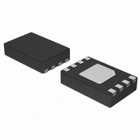
CAT5126VP2I10GT3 ON Semiconductor, CAT5126VP2I10GT3 Datasheet - Page 3

CAT5126VP2I10GT3
Manufacturer Part Number
CAT5126VP2I10GT3
Description
IC POT DPP OTP 32TAP U/D 8-TDFN
Manufacturer
ON Semiconductor
Datasheet
1.CAT5126ZI-10-GT3.pdf
(9 pages)
Specifications of CAT5126VP2I10GT3
Taps
32
Resistance (ohms)
50K
Number Of Circuits
1
Temperature Coefficient
50 ppm/°C Typical
Memory Type
Non-Volatile
Interface
I²C, 2-Wire Serial
Voltage - Supply
2.5 V ~ 5.5 V
Operating Temperature
-40°C ~ 85°C
Mounting Type
Surface Mount
Package / Case
8-VFDFN Exposed Pad
Resistance In Ohms
50K
Number Of Pots
Single
Taps Per Pot
32
Resistance
10 KOhms
Wiper Memory
Non Volatile
Digital Interface
Serial (2-Wire, I2C)
Operating Supply Voltage
5 V
Supply Current
5 uA
Maximum Operating Temperature
+ 85 C
Minimum Operating Temperature
- 40 C
Mounting Style
SMD/SMT
Supply Voltage (max)
5.5 V
Supply Voltage (min)
2.5 V
Lead Free Status / RoHS Status
Lead free / RoHS Compliant
Available stocks
Company
Part Number
Manufacturer
Quantity
Price
Company:
Part Number:
CAT5126VP2I10GT3
Manufacturer:
ON Semiconductor
Quantity:
2 150
Table 3. ELECTRICAL CHARACTERISTICS
unless otherwise noted. Typical values are at V
1. All devices are production tested at T
2. Digital inputs CS and U/D are connected to GND or V
3. Digital timing is guaranteed by design, not production tested.
4. Power−up time is the period of time from when the power supply is applied until the serial interface is ready for writing.
DC PERFORMANCE
DIGITAL INPUTS (CS, U/D)
POWER SUPPLY
TIMING CHARACTERISTICS (Note 3)
TC
Symbol
TC
f
U/DMAX
R
I
RES
DNL
V
V
DDW
INL
R
V
C
I
t
t
V
I
t
t
t
t
t
RATIO
I
t
t
t
POT
RPOT
DD
CU
t
PC
CP
CH
PH
PP
IW
CL
IN
DD
PP
CI
IC
IL
IH
IH
W
IL
IN
Resolution
End−to−End Resistance
TC of Pot Resistance
Ratiometric Resistance TC
Integral Nonlinearity
Differential Nonlinearity
Wiper Resistance
Input High Voltage
Input Low Voltage
Input Leakage Current
Input Capacitance
Supply Voltage
Stand by Current
Programming Current
Programming Voltage
V
U/D Mode to CS Setup
CS Hold to U/D Mode
U/D Step Hold to CS
U/D Step Low Time
U/D Step High Time
Wiper Switching Time
V
Falling Edge
CS Falling Edge to V
Falling Edge
CS Step Low Time
CS Step High Time
V
Rising Edge
U/D Frequency
PP
PP
PP
Input Current
Rising Edge to CS
Falling Edge to CS
Parameter
PP
A
= +25°C and are guaranteed by design for T
DD
Potentiometer configuration, no load
Potentiometer configuration, no load
= 5.0 V, T
(V
DD
C
L
DD
= 2.5 V to 5.5 V, V
http://onsemi.com
= 0 pF, Figures 6, 7
.
A
V
V
Conditions
Figures 6, 7
Figures 6, 7
Figures 6, 7
Figures 6, 7
Figures 6, 7
−10 Device
−50 Device
−00 Device
V
V
V
= +25°C, unless otherwise noted.) (Note 1)
DD
DD
Figure 8
Figure 8
Figure 8
Figure 8
Figure 8
(Note 2)
PP
DD
DD
= 2.5 V
= 2.5 V
= 10 V
= 5 V
= 5 V
3
PP
= GND, R
A
= −40°C to +85°C.
H
0.7 x V
= V
Min
100
100
2.5
40
80
50
50
8
0
1
5
5
5
1
DD
DD
, R
L
= GND, T
0.25
±0.1
0.35
0.25
Typ
100
±50
150
100
3.2
0.5
8.5
6.0
10
50
±5
70
5
A
= −40°C to +85°C,
0.3 x V
±300
Max
120
±20
100
200
0.5
5.5
12
60
10
10
±1
1
1
1
5
5
DD
ppm/°C
ppm/°C
Units
MHz
LSB
LSB
mA
kW
ms
ms
ms
ms
ms
mA
pF
mA
mA
ns
ns
ns
ns
ns
ns
%
W
V
V
V
V


