X9118TV14IZ-2.7 Intersil, X9118TV14IZ-2.7 Datasheet - Page 4

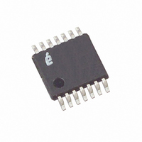
X9118TV14IZ-2.7
Manufacturer Part Number
X9118TV14IZ-2.7
Description
IC XDCP SGL 1024TAP 100K 14TSSOP
Manufacturer
Intersil
Series
XDCP™r
Datasheet
1.X9118TV14.pdf
(17 pages)
Specifications of X9118TV14IZ-2.7
Taps
1024
Resistance (ohms)
100K
Number Of Circuits
1
Temperature Coefficient
300 ppm/°C Typical
Memory Type
Non-Volatile
Interface
I²C, 2-Wire Serial
Voltage - Supply
2.7 V ~ 5.5 V
Operating Temperature
-40°C ~ 85°C
Mounting Type
Surface Mount
Package / Case
14-TSSOP
Resistance In Ohms
100K
Lead Free Status / RoHS Status
Lead free / RoHS Compliant
At both ends of each array and between each resistor
segment is a CMOS switch (transmission gate) connected to
the wiper (R
switch may be turned on at a time. These switches are
controlled by the Wiper Counter Register (WCR). The
10-bits of the WCR (WCR[9:0]) are decoded to select, and
enable, one of 1024 switches.
The WCR may be written directly. The Data Registers and
the WCR can be read and written by the host system.
Serial Interface Description
SERIAL INTERFACE – 2-WIRE
The X9118 supports a bidirectional bus oriented protocol.
The protocol defines any device that sends data onto the
bus as a transmitter and the receiving device as the receiver.
The device controlling the transfer is a master and the
device being controlled is the slave. The master will always
initiate data transfers and provide the clock for both transmit
and receive operations. Therefore, the X9118 will be
considered a slave device in all applications.
CLOCK AND DATA CONVENTIONS
Data states on the SDA line can change only during SCL
LOW periods. SDA state changes during SCL HIGH are
reserved for indicating start and stop conditions. See Figure 3.
If WCR = 000[HEX] then R
If WCR = 3FF[HEX] then R
FROM INTERFACE
SERIAL DATA PATH
CIRCUITRY
W
) output. Within each individual array only one
W
W
= R
= R
4
L
REGISTER 0
REGISTER 2
H
(DR0)
(DR2)
FIGURE 1. DETAILED POTENTIOMETER BLOCK DIAGRAM
10
REGISTER 1
REGISTER 3
(DR1)
(DR3)
X9118
10
START CONDITION
All commands to the X9118 are preceded by the start
condition, which is a HIGH to LOW transition of SDA while
SCL is HIGH. The X9118 continuously monitors the SDA
and SCL lines for the start condition and will not respond to
any command until this condition is met. See Figure 3.
STOP CONDITION
All communications must be terminated by a stop condition,
which is a LOW to HIGH transition of SDA while SCL is
HIGH. See Figure 3.
ACKNOWLEDGE
Acknowledge is a software convention used to provide a
positive handshake between the master and slave devices
on the bus to indicate the successful receipt of data. The
transmitting device, either the master or the slave, will
release the SDA bus after transmitting eight bits. The master
generates a ninth clock cycle and during this period the
receiver pulls the SDA line LOW to acknowledge that it
successfully received the eight bits of data.
The X9118 will respond with an acknowledge after
recognition of a start condition and its slave address and
once again after successful receipt of the command byte. If
the command is followed by a data byte, the X9118 will
respond with a final acknowledge. See Figure 2.
BUS
INPUT
SERIAL
BUS
INPUT
PARALLEL
REGISTER
COUNTER
WIPER
(WCR)
C
O
U
N
T
E
R
D
E
C
O
D
E
R H
R L
R
W
December 4, 2009
FN8161.4


