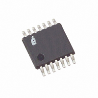
X9110TV14IZ Intersil, X9110TV14IZ Datasheet - Page 7

X9110TV14IZ
Manufacturer Part Number
X9110TV14IZ
Description
IC XDCP SGL 1024TAP 100K 14TSSOP
Manufacturer
Intersil
Series
XDCP™r
Datasheet
1.X9110TV14.pdf
(18 pages)
Specifications of X9110TV14IZ
Taps
1024
Resistance (ohms)
100K
Number Of Circuits
1
Temperature Coefficient
300 ppm/°C Typical
Memory Type
Non-Volatile
Interface
SPI, 3-Wire Serial
Voltage - Supply
4.5 V ~ 5.5 V
Operating Temperature
-40°C ~ 85°C
Mounting Type
Surface Mount
Package / Case
14-TSSOP
Resistance In Ohms
100K
Track Taper
Linear
Resistance Tolerance
± 20%
No. Of Steps
1024
Supply Voltage Range
4.5V To 5.5V
Control Interface
SPI
No. Of Pots
Single
Rohs Compliant
Yes
Lead Free Status / RoHS Status
Lead free / RoHS Compliant
Available stocks
Company
Part Number
Manufacturer
Quantity
Price
Company:
Part Number:
X9110TV14IZ-2.7
Manufacturer:
NJR
Quantity:
829
Write in Process (WIP bit)
The contents of the Data Registers are saved to nonvolatile
memory when the CS pin goes from LOW to HIGH after a
complete write sequence is received by the device. The
progress of this internal write operation can be monitored by
a Write In Process bit (WIP). The WIP bit is read with a Read
Status command (See Figure 4).
SCK
SCK
CS
SI
CS
SI
ID3 ID2 ID1 ID0 0
ID3 ID2 ID1 ID0 0
0
0
DEVICE ID
FIGURE 3. FOUR-BYTE INSTRUCTION SEQUENCE (WRITE OR READ FOR WCR OR DATA REGISTERS)
DEVICE ID
SCK
1
1
CS
SI
0
0
1
1
FIGURE 4. FOUR-BYTE INSTRUCTION SEQUENCE (READ STATUS REGISTERS)
0
0
INTERNAL
ADDRESS
INTERNAL
ADDRESS
0
0
0
7
ID3 ID2 ID1 ID0
A0 R/W I2
A0 R/W I2
0
0
1
DEVICE ID
INSTRUCTION
INSTRUCTION
1
OPCODE
OPCODE
FIGURE 2. TWO-BYTE INSTRUCTION SEQUENCE
I1 I0
I1 I0 0 RB RA
0
1
0
0
0 RB RA
ADDRESS
REGISTER
0
ADDRESS
0
REGISTER
X X 0
X X 0
0
0
INTERNAL
ADDRESS
0 0
0
A0
X9110
0
0
0
R/W
X X
X X
I2
X X X
Power-up and Down Requirements
At all times, the V+ voltage must be greater than or equal to
the voltage at R
greater than or equal to the voltage at V-. During power-up
and power-down, V
values within 1msec of each other.
X X
INSTRUCTION
OPCODE
I1
X
X
X
I0
W
C
R
9
X X
W
C
R
8
0
H
W
C
R
7
REGISTER
ADDRESS
0
or R
RB
W
C
R
6
CC
0
POSITION
L
WIPER
W
C
R
5
RA
, V+, and V- must reach their final
, and the voltage at R
0
W
C
R
4
0 0
0
W
C
R
3
0
W
C
R
2
0 0
0
0
W
C
R
1
STATUS
WIP
W
C
R
0
BIT
H
or R
February 13, 2008
L
must be
FN8158.3


