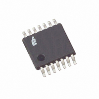
X9429YV14IZ-2.7T1 Intersil, X9429YV14IZ-2.7T1 Datasheet - Page 13

X9429YV14IZ-2.7T1
Manufacturer Part Number
X9429YV14IZ-2.7T1
Description
IC XDCP SGL 64-TAP 2.5K 14-TSSOP
Manufacturer
Intersil
Series
XDCP™r
Datasheet
1.X9429WS16ZT1.pdf
(20 pages)
Specifications of X9429YV14IZ-2.7T1
Taps
64
Resistance (ohms)
2.5K
Number Of Circuits
1
Temperature Coefficient
300 ppm/°C Typical
Memory Type
Non-Volatile
Interface
I²C, 2-Wire Serial
Voltage - Supply
2.7 V ~ 5.5 V
Operating Temperature
-40°C ~ 85°C
Mounting Type
Surface Mount
Package / Case
14-TSSOP
Resistance In Ohms
2.5K
Lead Free Status / RoHS Status
Lead free / RoHS Compliant
ENDURANCE AND DATA RETENTION
CAPACITANCE
POWER-UP TIMING
NOTES:
Power-up and Power-down Requirements
There are no restrictions on the power-up or power-down
conditions of V
potentiometer pins provided that V
positive than or equal to V
V
Equivalent AC Load Circuit
Minimum Endurance
Data Retention
1. Absolute linearity is utilized to determine actual wiper voltage versus expected voltage as determined by wiper position when used as a
2. Relative linearity is utilized to determine the actual change in voltage between two successive tap positions when used as a potentiometer. It is
3. MI = RTOT/63 or (R
4. Typical = individual array resolutions.
5. Limits established by characterization and are not production tested.
6. Sample tested only.
7. Parts are 100% tested at +25°C. Over temperature limits established by characterization and are not production tested.
W
t
C
SYMBOL
C
R
. The V
SYMBOL
I/O
potentiometer.
a measure of the error in step size.
V
IN
SYMBOL
V
V
CC
I
V
LO
(Note 5)
OL
(Note 5)
SDA OUTPUT
IH
IL
(Note 6)
CC
ramp rate spec is always in effect.
Output Leakage Current
Input HIGH Voltage
Input LOW Voltage
Output LOW voltage
CC
PARAMETER
Input/output capacitance (SDA)
Input capacitance (A0, A2,and A3 and SCL)
and the voltage applied to the
V
CC
H
Power-up ramp rate
- R
PARAMETER
L
H
5V
)/63, single pot
, V
13
1533Ω
100pF
L
, and V
CC
is always more
PARAMETER
W
, i.e., V
TEST
2.7V
CC
V
I
OL
100pF
OUT
≥ V
100,000
= 3mA
MIN.
100
= V
H
TEST CONDITIONS
, V
SS
L
,
to V
X9429
CC
Data changes per bit per register
Years
AC Test Conditions
Circuit #3 SPICE Macro Model
Input pulse levels
Input rise and fall times
Input and output timing level
R
H
MIN
0.2
TYP
8
6
10pF
V
(Note 7)
C
CC
MIN.
H
-0.5
x 0.7
R
TOTAL
TYP
R
W
25pF
UNIT
C
UNIT
pF
pF
W
TYP
LIMITS
10pF
C
L
MAX
V
10ns
V
50
CC
CC
V
V
(Note 7)
TEST CONDITIONS
R
x 0.1 to V
x 0.5
CC
CC
MAX.
L
0.4
10
x 0.5
x 0.1
V
V
I/O
IN
= 0V
CC
= 0V
October 13, 2008
UNIT
V/ms
x 0.9
UNIT
FN8248.3
µA
V
V
V


