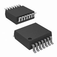
ISL22449WFV14Z-TK Intersil, ISL22449WFV14Z-TK Datasheet - Page 10

ISL22449WFV14Z-TK
Manufacturer Part Number
ISL22449WFV14Z-TK
Description
IC POT DGTL 128TP LN LP 14-TSSOP
Manufacturer
Intersil
Series
XDCP™r
Datasheet
1.ISL22449WFV14Z.pdf
(13 pages)
Specifications of ISL22449WFV14Z-TK
Taps
128
Resistance (ohms)
10K
Number Of Circuits
4
Temperature Coefficient
50 ppm/°C Typical
Memory Type
Non-Volatile
Interface
SPI, 3-Wire Serial
Voltage - Supply
2.7 V ~ 5.5 V
Operating Temperature
-40°C ~ 125°C
Mounting Type
Surface Mount
Package / Case
14-TSSOP
Resistance In Ohms
10K
Lead Free Status / RoHS Status
Lead free / RoHS Compliant
SPI Serial Interface
The ISL22449 supports an SPI serial protocol, mode 0. The
device is accessed via the SDI input and SDO output with
data clocked in on the rising edge of SCK, and clocked out
on the falling edge of SCK. CS must be LOW during
communication with the ISL22449. SCK and CS lines are
controlled by the host or master. The ISL22449 operates
only as a slave device.
All communication over the SPI interface is conducted by
sending the MSB of each byte of data first.
Protocol Conventions
The first byte sent to the ISL22449 from the SPI host is the
Identification Byte. A valid Identification Byte contains 0101
as the four MSBs, with the following four bits set to 0.
The next byte sent to the ISL22449 contains the instruction
and register pointer information. The four MSBs are the
instruction and four LSBs are register address (see Table 5).
There are only two valid instruction sets:
1011(binary) - is a Read operation
1100(binary) - is a Write operation
(MSB)
I3
0
7
SHDN pin
High
High
Low
Low
TABLE 4. IDENTIFICATION BYTE FORMAT
TABLE 5. IDENTIFICATION BYTE FORMAT
I2
1
6
I1
0
5
SHDN bit
I0
1
1
0
0
TABLE 3.
1
4
10
R3
0
3
Normal operation
R2
0
2
Shutdown
Shutdown
Shutdown
Mode
R1
0
1
(LSB)
R0
0
0
ISL22449
Write Operation
A Write operation to the ISL22449 is a three-byte operation. It
requires first, the CS transition from HIGH to LOW, then a valid
Identification Byte, then a valid instruction byte following by
Data Byte is sent to SDI pin. The host terminates the write
operation by pulling the CS pin from LOW to HIGH. For a write
to addresses 0000b to 0011b, the MSB at address 8 (ACR[7])
determines if the Data Byte is to be written to volatile or both
volatile and non-volatile registers. Refer to “Memory
Description” on page 9 and Figure 12.
Device can receive more than one byte of data by auto
incrementing the address after each received byte. Note
after reaching the address 0110b, the internal pointer “rolls
over” to address 0000b.
The internal non-volatile write cycle starts after rising edge of
CS and takes up to 20ms. Thus, non-volatile registers must
be written individually.
Read Operation
A read operation to the ISL22449 is a three-byte operation. It
requires first, the CS transition from HIGH to LOW, then a
valid Identification Byte, then a valid instruction byte
following by “dummy” Data Byte is sent to SDI pin. The SPI
host reads the data from SDO pin on falling edge of SCK.
The host terminates the read operation by pulling the CS pin
from LOW to HIGH (see Figure 13).
The ISL22449 will provide the Data Bytes to the SDO pin as
long as SCK is provided by the host from the registers
indicated by an internal pointer. This pointer initial value is
determined by the register address in the Read operation
instruction, and increments by one during transmission of
each Data Byte. After reaching the memory location 0110b,
the pointer “rolls over” to 0000b, and the device continues to
output the data for each received SCK clock.
In order to read back the non-volatile IVR, it is recommended
that the application reads the ACR first to verify the WIP bit
is 0. If the WIP bit (ACR[5]) is not 0, the host should repeat
its reading sequence again.
July 17, 2009
FN6333.3


