ISL23711WIU10Z Intersil, ISL23711WIU10Z Datasheet
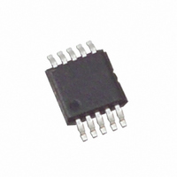
IC INTERFACE XDCP 10-MSOP

ISL23711WIU10Z

Manufacturer Part Number
ISL23711WIU10Z
Description
IC INTERFACE XDCP 10-MSOP
Manufacturer
Intersil
Series
XDCP™r
Datasheet

Specifications of ISL23711WIU10Z

Taps
128
Resistance (ohms)
10K
Number Of Circuits
1
Temperature Coefficient
50 ppm/°C Typical
Memory Type
Volatile
Interface
I²C, 2-Wire Serial
Voltage - Supply
2.7 V ~ 5.5 V
Operating Temperature
-40°C ~ 85°C
Mounting Type
Surface Mount
Package / Case
10-MSOP, Micro10™, 10-uMAX, 10-uSOP
Resistance In Ohms
10K
Lead Free Status / RoHS Status
Lead free / RoHS Compliant

Available stocks

Company
Part Number
Manufacturer
Quantity
Price
Part Number:
ISL23711WIU10Z-T
Manufacturer:
INTERSIL
Quantity:
101
Part Number:
ISL23711WIU10Z-T
Manufacturer:
Intersil
Quantity:
70
Terminal Voltage ±3V or ±5V, 128 Taps I
Serial Interface
The Intersil ISL23711 is a digitally controlled potentiometer
(XDCP). The device consists of a resistor array, wiper
switches, and a control section. The wiper position is
controlled by an I
The potentiometer is implemented by a resistor array
composed of 127 resistive elements and a wiper switching
network. The wiper terminal can be connected to either end
of the resistor array or at any one of the Tap Positions in
between, providing 128 steps of resolution between R
R
assigned to the volatile Wiper Register (WR). The WR can
be directly written to and read from using standard I
interface protocol. The device is available in either a 10kΩ or
50kΩ version.
The device can be used as a three-terminal potentiometer or
as a two-terminal variable resistor in a wide variety of
applications including:
• Industrial and Automotive Control
• Parameter and Bias Adjustments
• Amplifier Bias and Control
Ordering Information
NOTES:
ISL23711WIU10Z
(AOE) (Notes 1, 2)
ISL23711UIU10Z
(AOD) (Notes 1, 2)
1. Add “-T” suffix for tape and reel.
2. Intersil Pb-free plus anneal products employ special Pb-free material
PART NUMBER
H
. The “position” of the wiper is determined by the value
sets; molding compounds/die attach materials and 100% matte tin plate
termination finish, which are RoHS compliant and compatible with both
SnPb and Pb-free soldering operations. Intersil Pb-free products are
MSL classified at Pb-free peak reflow temperatures that meet or
exceed the Pb-free requirements of IPC/JEDEC J STD-020.
(BRAND)
2
C interface.
RESISTANCE
OPTION (Ω)
10K
50K
®
1
-40 to +85 10 Ld MSOP
RANGE
TEMP
(°C)
Data Sheet
PACKAGE
(Pb-Free)
(Pb-Free)
2
C
Volatile Digitally Controlled Potentiometer (XDCP™)
L
1-888-INTERSIL or 1-888-468-3774 | Intersil (and design) is a registered trademark of Intersil Americas Inc.
and
2
C
CAUTION: These devices are sensitive to electrostatic discharge; follow proper IC Handling Procedures.
M10.118
M10.118
DWG. #
PKG.
XDCP is a trademark of Intersil, Inc. Copyright Intersil Americas Inc. 2005. All Rights Reserved
Features
• I
• DCP Terminal Voltage, from V- to V
• 127 Resistive Elements
• Low Power CMOS
• R
• Volatile Wiper Storage
• Package
• Pb-Free Plus Anneal Available (RoHS Compliant)
Pinout
up to Four Devices
- Typical R
- Typical ratiometric tempco ±4ppm/
- End to end resistance range ±20%
- Wiper resistance = 70Ω typ at V
- Standby current, 500nA max
- Active current, 200µA max
- V
- V- = -2.7V to -5.5V
- 10 Ld MSOP
2
TOTAL
C Serial Interface with Hardwire Slave Address Allows
August 16, 2005
CC
All other trademarks mentioned are the property of their respective owners.
= 2.7V to 5.5V
Values = 10kΩ, 50kΩ
TOTAL
GND
SDA
A1
A0
V-
tempco ±50ppm/
1
2
3
4
5
(10 LD MSOP)
TOP VIEW
ISL23711
10
9
8
7
6
CC
CC
°
C
°
C
= 3.3V
ISL23711
SCL
V
R
R
R
CC
W
L
H
FN6127.0

Related parts for ISL23711WIU10Z

ISL23711WIU10Z Summary of contents

Page 1

... Parameter and Bias Adjustments • Amplifier Bias and Control Ordering Information TEMP PART NUMBER RESISTANCE RANGE (BRAND) OPTION (Ω) (°C) ISL23711WIU10Z 10K - MSOP (AOE) (Notes 1, 2) ISL23711UIU10Z 50K - MSOP (AOD) (Notes 1, 2) NOTES: 1. Add “-T” suffix for tape and reel. ...

Page 2

Block Diagram V GND CC SDA R SCL INTERFACE R AND A1 CONTROL SIMPLE BLOCK DIAGRAM Pin Descriptions PIN NUMBER SYMBOL 1 SDA GND ...

Page 3

Absolute Maximum Ratings Temperature under bias . . . . . . . . . . . . . . . . . . . . . .-65°C to +135°C Storage temperature . . . . . . . . ...

Page 4

Operating Specifications Over the recommended operating conditions unless otherwise specified. SYMBOL PARAMETER I V Supply Current, Volatile CC1 CC Write/Read I V- Supply Current, Volatile Write/Read Current (Standby Current (Standby) V-SB I ...

Page 5

Operating Specifications Over the recommended operating conditions unless otherwise specified. (Continued) SYMBOL PARAMETER t Output Data Hold Time DH t SDA, SCL, A0, A1 Rise Time R (Note 14) t SDA, SCL, A0, A1 Fall Time F (Note 14) Cb ...

Page 6

NOTES: ± 1. Typical values are for T = 25°C and A 2. LSB: [V(RW) – V(RW 127. V(RW) 127 0 incremental voltage when changing from one tap to an adjacent tap error = (V(RW) – ...

Page 7

At either end of the array and between each resistor is an electronic switch that transfers the potential at that point to the wiper. The wiper, when at either fixed terminal, acts like ...

Page 8

SCL SDA START FIGURE 1. VALID DATA CHANGES, START, AND STOP CONDITIONS SCL FROM MASTER SDA OUTPUT FROM TRANSMITTER HIGH IMPEDANCE SDA OUTPUT FROM RECEIVER START FIGURE 2. ACKNOWLEDGE RESPONSE FROM RECEIVER S SIGNALS FROM T THE MASTER A IDENTIFICATION ...

Page 9

... Accordingly, the reader is cautioned to verify that data sheets are current before placing orders. Information furnished by Intersil is believed to be accurate and reliable. However, no responsibility is assumed by Intersil or its subsidiaries for its use; nor for any infringements of patents or other rights of third parties which may result from its use ...

Related keywords