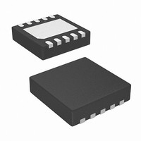
ISL22316UFRT10Z Intersil, ISL22316UFRT10Z Datasheet

ISL22316UFRT10Z
Specifications of ISL22316UFRT10Z
Available stocks
Related parts for ISL22316UFRT10Z
ISL22316UFRT10Z Summary of contents
Page 1
... MARKING ISL22316UFU10Z* 316UZ ISL22316WFU10Z* 316WZ ISL22316UFRT10Z* 316U ISL22316WFRT10Z* 316W *Add “-TK” suffix for tape and reel. Please refer to TB347 for details on reel specifications. NOTE: These Intersil Pb-free plastic packaged products employ special Pb-free material sets, molding compounds/die attach materials, and 100% matte tin plate plus anneal (e3 termination finish, which is RoHS compliant and compatible with both SnPb and Pb-free soldering operations) ...
Page 2
Block Diagram SCL SDA A0 INTERFACE A1 SHDN Pin Descriptions MSOP PIN TDFN PIN NUMBER NUMBER ISL22316 V CC ...
Page 3
... Thermal Resistance (Typical) 10 Lead MSOP (Note 2 +0 Lead TDFN (Notes Maximum Junction Temperature (Plastic Package +150°C Pb-free Reflow Profile . . . . . . . . . . . . . . . . . . . . . . . . .see link below http://www.intersil.com/pbfree/Pb-FreeReflow.asp CC Recommended Operating Conditions Temperature Range (Extended Industrial .-40°C to +125° Power Rating of each DCP . . . . . . . . . . . . . . . . . . . . . . . . . . . .5mW Wiper Current of each DCP . . . . . . . . . . . . . . . . . . . . . . . . . . ±3.0mA ...
Page 4
Analog Specifications Over recommended operating conditions, unless otherwise stated. (Continued) SYMBOL PARAMETER RESISTOR MODE (Measurements between R RINL Integral Non-linearity (Note 15) RDNL Differential Non-linearity (Note 14) Roffset Offset (Note 13) Operating Specifications Over the recommended operating conditions, unless otherwise ...
Page 5
Operating Specifications Over the recommended operating conditions, unless otherwise specified. (Continued) SYMBOL PARAMETER EEPROM SPECIFICATION EEPROM Endurance EEPROM Retention t Non-volatile Write Cycle Time WC (Note 17) SERIAL INTERFACE SPECIFICATIONS V A1, A0, SHDN, SDA, and SCL Input Buffer IL ...
Page 6
Operating Specifications Over the recommended operating conditions, unless otherwise specified. (Continued) SYMBOL PARAMETER Rpu SDA and SCL Bus Pull-up Resistor Off-chip Maximum is determined and A0 Setup Time SU and A0 Hold Time HD:A ...
Page 7
SDA vs SCL Timing SCL t SU:STA t HD:STA SDA (INPUT TIMING) SDA (OUTPUT TIMING) A0 and A1 Pin Timing START SCL SDA A0, A1 Typical Performance Curves 100 V = 3.3V +125° ...
Page 8
Typical Performance Curves 0 2.7V CC 0 5. TAP POSITION (DECIMAL) FIGURE 3. DNL vs TAP POSITION IN VOLTAGE DIVIDER MODE FOR 10kΩ (W) 1.3 10k 1.1 0.9 ...
Page 9
Typical Performance Curves 1.0 0 2. 5.5V CC 10k -0.5 -1.0 -40 - TEMPERATURE (ºC) FIGURE 9. END-TO-END R % CHANGE vs TOTAL TEMPERATURE 300 250 200 150 50k 100 50 ...
Page 10
Pin Description Potentiometers Pins RH AND RL The high (RH) and low (RL) terminals of the ISL22316 are equivalent to the fixed terminals of a mechanical potentiometer. RH and RL are referenced to the relative position of the wiper and ...
Page 11
TABLE 1. MEMORY MAP ADDRESS NON-VOLATILE 2 — 1 Reserved 0 IVR The non-volatile IVR and volatile WR registers are accessible with ...
Page 12
SCL SDA START FIGURE 16. VALID DATA CHANGES, START AND STOP CONDITIONS SCL FROM MASTER SDA OUTPUT FROM TRANSMITTER HIGH IMPEDANCE SDA OUTPUT FROM RECEIVER START FIGURE 17. ACKNOWLEDGE RESPONSE FROM RECEIVER SIGNALS FROM THE MASTER SIGNAL AT SDA SIGNALS ...
Page 13
Write Operation A Write operation requires a START condition, followed by a valid Identification Byte, a valid Address Byte, a Data Byte, and a STOP condition. After each of the three bytes, the ISL22316 responds with an ACK. At this ...
Page 14
... Dimensions D2 and E2 are for the exposed pads which provide improved electrical and thermal performance Nominal dimensions are provided to assist with PCB Land Pattern Design efforts, see Intersil Technical Brief TB389. 9. COMPLIANT TO JEDEC MO-229-WEED-3 except for dimensions E2 & D2 TERMINAL TIP MILLIMETERS MIN NOMINAL MAX 0 ...
Page 15
... Accordingly, the reader is cautioned to verify that data sheets are current before placing orders. Information furnished by Intersil is believed to be accurate and reliable. However, no responsibility is assumed by Intersil or its subsidiaries for its use; nor for any infringements of patents or other rights of third parties which may result from its use ...


