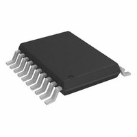
AD5254BRUZ50 Analog Devices Inc, AD5254BRUZ50 Datasheet - Page 9

AD5254BRUZ50
Manufacturer Part Number
AD5254BRUZ50
Description
IC POT DGTL QUAD 50K 20TSSOP
Manufacturer
Analog Devices Inc
Datasheet
1.AD5254BRUZ100.pdf
(32 pages)
Specifications of AD5254BRUZ50
Memory Type
Non-Volatile
Temperature Coefficient
650 ppm/°C Typical
Taps
256
Resistance (ohms)
50K
Number Of Circuits
4
Interface
I²C, 2-Wire Serial
Voltage - Supply
2.7 V ~ 5.5 V, ±2.25 V ~ 2.75 V
Operating Temperature
-40°C ~ 85°C
Mounting Type
Surface Mount
Package / Case
20-TSSOP
Resistance In Ohms
50K
End To End Resistance
50kohm
Track Taper
Linear
Resistance Tolerance
± 30%
No. Of Steps
256
No. Of Pots
Quad
Potentiometer Ic Case
RoHS Compliant
Supply Voltage Range
± 2.25V To ± 2.75V
Control Interface
I2C, Serial
Rohs Compliant
Yes
Lead Free Status / RoHS Status
Lead free / RoHS Compliant
For Use With
AD5254EVAL - BOARD EVAL FOR AD5254
Lead Free Status / RoHS Status
Lead free / RoHS Compliant
Available stocks
Company
Part Number
Manufacturer
Quantity
Price
Part Number:
AD5254BRUZ50
Manufacturer:
ADI/亚德诺
Quantity:
20 000
PIN CONFIGURATION AND FUNCTION DESCRIPTIONS
Table 5. Pin Function Descriptions
Pin No.
1
2
3
4
5
6
7
8
9
10
11
12
13
14
15
16
17
18
19
20
Mnemonic
W0
B0
A0
AD0
WP
W1
B1
A1
SDA
V
A2
B2
W2
SCL
DGND
AD1
A3
B3
W3
V
SS
DD
Description
Wiper Terminal of RDAC0. V
B Terminal of RDAC0. V
A Terminal of RDAC0. V
I
Write Protect, Active Low. V
Wiper Terminal of RDAC1. V
B Terminal of RDAC1. V
A Terminal of RDAC1. V
Serial Data Input/Output Pin. Shifts in one bit at a time upon positive clock edges. MSB loaded first. Open-drain
MOSFET requires pull-up resistor.
Negative Supply. Connect to 0 V for single supply or –2.7 V for dual supply, where V
rather than grounded in dual supply, V
A Terminal of RDAC2. V
B Terminal of RDAC2. V
Wiper Terminal of RDAC2. V
Serial Input Register Clock Pin. Shifts in one bit at a time upon positive clock edges. V
resistor is recommended for SCL to ensure minimum power.
Digital Ground. Connect to system analog ground at a single point.
I
A Terminal of RDAC3. V
B Terminal of RDAC3. V
Wiper Terminal of RDAC3. V
Positive Power Supply Pin. Connect +2.7 V to +5 V for single supply or ±2.7 V for dual supply, where V
V
2
2
C Device Address 0. AD0 and AD1 allow four AD5253/AD5254 devices to be addressed.
C Device Address 1. AD0 and AD1 allow four AD5253/AD5254 devices to be addressed.
DD
must be able to source 35 mA for 26 ms when storing data to EEMEM.
SS
SS
SS
SS
SS
SS
SS
SS
≤ V
≤ V
≤ V
≤ V
≤ V
≤ V
≤ V
≤ V
SS
WP
SS
SS
SS
B0
B1
B2
B3
A0
A1
A2
A3
SDA
AD0
≤ V
≤ V
≤ V
≤ V
V
WP
W0
W1
≤ V
≤ V
≤ V
≤ V
≤ V
B0
A0
B1
A1
≤ V
≤ V
≤ V
≤ V
SS 10
Figure 2. Pin Configuration
W0
W1
W2
W3
DD
DD
DD
DD
DD
DD
DD
DD
DD
1
2
3
4
5
6
7
8
9
Rev. B | Page 9 of 32
≤ V
≤ V
≤ V
≤ V
.
.
.
.
.
+ 0.3 V.
.
.
.
(Not to Scale)
AD5253/
AD5254
TOP VIEW
DD
DD
DD
DD
SS
.
.
.
.
must be able to sink 35 mA for 26 ms when storing data to EEMEM.
20
19
18
17
16
15
14
13
12
11
V
W3
B3
A3
AD1
DGND
SCL
W2
B2
A2
DD
DD
SCL
– V
AD5253/AD5254
≤ (V
SS
≤ +5.5 V. If V
DD
+ 0.3 V). Pull-up
DD
– V
SS
SS
≤ +5.5 V.
is used


