AD5252BRUZ100 Analog Devices Inc, AD5252BRUZ100 Datasheet - Page 9
AD5252BRUZ100
Manufacturer Part Number
AD5252BRUZ100
Description
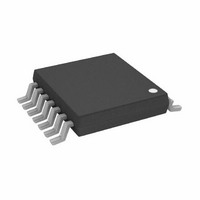
IC DIG POT DUAL 256 100K 14TSSOP
Manufacturer
Analog Devices Inc
Datasheet
1.AD5252BRUZ10.pdf
(28 pages)
Specifications of AD5252BRUZ100
Taps
256
Resistance (ohms)
100K
Number Of Circuits
2
Temperature Coefficient
650 ppm/°C Typical
Memory Type
Non-Volatile
Interface
I²C, 2-Wire Serial
Voltage - Supply
2.7 V ~ 5.5 V, ±2.25 V ~ 2.75 V
Operating Temperature
-40°C ~ 85°C
Mounting Type
Surface Mount
Package / Case
14-TSSOP
Resistance In Ohms
100K
End To End Resistance
100kohm
Track Taper
Linear
Resistance Tolerance
± 20%
No. Of Steps
256
Supply Voltage Range
2.7V To 5.5V, ± 2.25V To ± 2.75V
Control Interface
I2C, Serial
Lead Free Status / RoHS Status
Lead free / RoHS Compliant
For Use With
AD5252EVAL - BOARD EVAL FOR AD5252
Lead Free Status / RoHS Status
Lead free / RoHS Compliant, Lead free / RoHS Compliant
Available stocks
Company
Part Number
Manufacturer
Quantity
Price
Company:

Part Number:
AD5252BRUZ100
Manufacturer:
Analog Devices Inc
Quantity:
135
Company:
Part Number:
AD5252BRUZ100
Manufacturer:
ADI
Quantity:
3 529


PIN CONFIGURATION AND FUNCTION DESCRIPTIONS
Table 5. Pin Function Descriptions
Pin No.
1
2
3
4
5
6
7
8
9
10
11
12
13
14
1
For quad-channel device software compatibility, the dual potentiometers in the parts are designated as RDAC1 and RDAC3.
Mnemonic
V
AD0
WP
W1
B1
A1
SDA
V
SCL
DGND
AD1
A3
B3
W3
DD
SS
I
Wiper Terminal of RDAC1. V
A Terminal of RDAC1. V
V
Digital Ground. Connect to system analog ground at a single point.
A Terminal of RDAC3. V
B Terminal of RDAC3. V
Wiper Terminal of RDAC3. V
Description
Positive Power Supply Pin. Connect +2.7 V to +5 V for single supply or ±2.7 V for dual supply, where
V
Write Protect, Active Low. V
B Terminal of RDAC1. V
Serial Data Input/Output Pin. Shifts in one bit at a time upon positive clock edges. MSB loaded first.
Open-drain MOSFET requires pull-up resistor.
Negative Supply. Connect to 0 V for single supply or –2.7 V for dual supply, where V
Serial Input Register Clock Pin. Shifts in one bit at a time upon positive clock edges. V
Pull-up resistor is recommended for SCL to ensure minimum power.
I
2
2
DD
C Device Address 0. AD0 and AD1 allow four AD5251/AD5252 devices to be addressed.
SS
C Device Address 1. AD0 and AD1 allow four AD5251/AD5252 devices to be addressed.
is used in dual supply, V
– V
SS
≤ 5.5 V. V
SDA
AD0
V
WP
W1
DD
B1
A1
DD
must be able to source 35 mA for 26 ms when storing data to EEMEM.
Figure 2. Pin Configuration
1
2
3
4
5
6
7
SS
SS
SS
SS
Rev. B | Page 9 of 28
≤ V
≤ V
(Not to Scale)
≤ V
≤ V
AD5251/
AD5252
TOP VIEW
SS
WP
SS
SS
B1
B3
A1
A3
must be able to sink 35 mA for 26 ms when storing data to EEMEM.
≤ V
≤ V
≤ V
≤ V
≤ V
≤ V
≤ V
W1
W3
DD
DD
DD
DD
DD
≤ V
.
.
≤ V
.
.
+ 0.3 V.
1
1
1
1
14
13
12
11
10
9
8
DD
DD
W3
B3
A3
AD1
DGND
SCL
V
.
.
1
1
SS
AD5251/AD5252
DD
SCL
– V
≤ (V
SS
≤ +5.5 V. If
DD
+ 0.3 V).
Related parts for AD5252BRUZ100
Image
Part Number
Description
Manufacturer
Datasheet
Request
R

Part Number:
Description:
±1.7g Dual-Axis IMEMS Accelerometer Evaluation Board
Manufacturer:
Analog Devices Inc
Datasheet:

Part Number:
Description:
Inertial Sensor Evaluation System
Manufacturer:
Analog Devices Inc
Datasheet:
Part Number:
Description:
Manufacturer:
Analog Devices Inc
Datasheet:
Part Number:
Description:
Manufacturer:
Analog Devices Inc
Datasheet:
Part Number:
Description:
Manufacturer:
Analog Devices Inc
Datasheet:
Part Number:
Description:
Manufacturer:
Analog Devices Inc
Datasheet:
Part Number:
Description:
Manufacturer:
Analog Devices Inc
Datasheet:
Part Number:
Description:
Manufacturer:
Analog Devices Inc
Datasheet:
Part Number:
Description:
Manufacturer:
Analog Devices Inc
Datasheet:
Part Number:
Description:
Manufacturer:
Analog Devices Inc
Datasheet:
Part Number:
Description:
Manufacturer:
Analog Devices Inc
Datasheet:
Part Number:
Description:
Manufacturer:
Analog Devices Inc
Datasheet:
Part Number:
Description:
Manufacturer:
Analog Devices Inc
Datasheet: