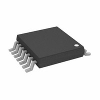
AD5207BRU10 Analog Devices Inc, AD5207BRU10 Datasheet - Page 9

AD5207BRU10
Manufacturer Part Number
AD5207BRU10
Description
IC DGTL POT DUAL 256POS 14TSSOP
Manufacturer
Analog Devices Inc
Datasheet
1.AD5207BRUZ100.pdf
(16 pages)
Specifications of AD5207BRU10
Mounting Type
Surface Mount
Package / Case
14-TSSOP
Rohs Status
RoHS non-compliant
Taps
256
Resistance (ohms)
10K
Number Of Circuits
2
Temperature Coefficient
500 ppm/°C Typical
Memory Type
Volatile
Interface
SPI, 3-Wire Serial
Voltage - Supply
2.7 V ~ 5.5 V, ±2.2 V ~ 2.7 V
Operating Temperature
-40°C ~ 125°C
Resistance In Ohms
10K
Peak Reflow Compatible (260 C)
No
Supply Voltage Max
5.5V
Leaded Process Compatible
No
Supply Voltage Min
2.7V
Wiper Type
Volatile
Lead Free Status / RoHS Status
Contains lead / RoHS non-compliant
Available stocks
Company
Part Number
Manufacturer
Quantity
Price
Part Number:
AD5207BRU100
Manufacturer:
ADI/亚德诺
Quantity:
20 000
OPERATION
The AD5207 provides a dual channel, 256-position digitally
controlled variable resistor (VR) device. The terms VR, RDAC,
and digital potentiometer are sometimes used interchangeably.
Changing the programmable VR settings is accomplished by
clocking in a 10-bit serial data word into the SDI (Serial Data
Input) pin. The format of this data word is two address Bits, A1
and A0. With A1 and A2 are first and second bits respectively,
followed by eight data bits B7–B0 with MSB first. Table I pro-
vides the serial register data word format. See Table III for the
AD5207 address assignments to decode the location of VR latch
receiving the serial register data in Bits B7 through B0. VR settings
can be changed one at a time in random sequence. The AD5207
presets to a midscale during power-on condition. AD5207 contains
a power shutdown SHDN pin. When activated in logic low.
Terminals A on both RDACs will be open-circuited while the
wiper terminals W
amount of leakage current will be consumed in both RDACs,
and the power dissipation is negligible. During the shutdown
mode, the VR latch settings are maintained. Thus the previ-
ous resistance values remain when the devices are resumed
from the shutdown.
DIGITAL INTERFACING
The AD5207 contains a standard three-wire serial input control
interface. The three inputs are clock (CLK), chip select (CS),
and serial data input (SDI). The positive edge-sensitive CLK
input requires clean transitions to avoid clocking incorrect data
into the serial input register. Standard logic families work well.
If mechanical switches are used for product evaluation, they
should be debounced by a flip-flop or other suitable means. Fig-
ure 2 shows more detail of the internal digital circuitry. When CS
is low, the clock loads data into the serial register on each posi-
tive clock edge; see Table II.
SDO
CLK
SDI
CS
AD5207
SER
REG
A0
D7
D6
D5
D4
D3
D2
D1
D0
X
ADDR
DEC
are shorted to B
EN
POWER-ON RESET
X
. As a result, a minimum
LATCH
LATCH
RDAC
RDAC
#1
#2
SHDN
V
A1
W1
B1
A2
W2
B2
V
DD
SS
The serial-data-output (SDO) pin contains an open drain
n-channel FET. This output requires a pull-up resistor in order
to transfer data to the next package’s SDI pin. The pull-up
resistor termination voltage may be larger than the V
of the AD5207 SDO output device, e.g., the AD5207 could
operate at V
device could be set at 5 V. This allows for daisy chaining several
RDACs from a single processor serial-data line. The clock period
may need to be increased when using a pull-up resistor to the
SDI pin of the following devices in series. Capacitive loading at
the daisy chain node SDO–SDI between devices may add time
delay to subsequent devices. User should be aware of this poten-
tial problem in order to successfully achieve data transfer. See
Figure 3. When configuring devices for daisy-chaining, the CS
should be kept low until all the bits of every package are clocked
into their respective serial registers, ensuring that the address bit
and data bits are in the proper decoding location. This requires
20 bits of address and data complying with the data word in
Table I if two AD5207 RDACs are daisy chained. During shut-
down SHDN, the SDO output pin is forced to OFF (logic high
state) to disable power dissipation in the pull-up resistor. See
Figure 4 for equivalent SDO output circuit schematic.
CLK CS
L
P
X
X
X
NOTE
P = positive edge, X = don’t care, SR = shift register.
C
L
L
P
H
H
Table II. Input Logic Control Truth Table
DD
SDI
SHDN
H
H
H
H
L
A1
0
0
Table III. Address Decode Table
= 3.3 V and the pull-up for interface to the next
CS
AD5207
CLK
A0
0
1
Register Activity
No SR effect, enables SDO pin.
Shift one bit in from the SDI pin. MSB
first. The tenth previously entered bit
is shifted out of the SDO pin.
Load SR data into RDAC latch based
on A0 decode (Table III).
No Operation.
Open circuits all resistor A Terminals,
connects W to B, turns off SDO out-
put transistor.
SDO
+V
Latch Loaded
RDAC #1
RDAC #2
R
2k
P
SDI
CS
AD5207
AD5207
CLK
DD
SDO
supply


